One of the future technologies, yes. As I said, the trend is to dump more features to the pixel level.
Reading mode:
Install the app
How to install the app on iOS
Follow along with the video below to see how to install our site as a web app on your home screen.
Note: This feature may not be available in some browsers.
-
Welcome to the new forums! Please read this first. For known issues we are working to resolve, click here.
You are using an out of date browser. It may not display this or other websites correctly.
You should upgrade or use an alternative browser.
You should upgrade or use an alternative browser.
Sensor size, complexity, pixel size and cost?
- Thread starter Erik Kaffehr
- Start date
bobn2
Forum Pro
That's one of the reasons they're pursuing stacking, but at present, the inter-chip vias are quite large, and I suspect yield is quite low if there are too many connections. It's one of those areas that's not so much a case of invention as development.
Large to the point they are impractical for small cameraphone pixels, and that depletes money needed for fast and successful intensive R&D.That's one of the reasons they're pursuing stacking, but at present, the inter-chip vias are quite large, and I suspect yield is quite low if there are too many connections. It's one of those areas that's not so much a case of invention as development.
Erik Kaffehr
Veteran Member
Hi,The big dilemma is this: to put serious money into R&D to improve the current generation of sensors, or to put it into R&D aimed at newer technologies.Hi,
It would be interesting to hear from folks knowledgeable about the cost aspects of modern sensor designs.
My understanding is that increasing the sensor size over proportionally expensive.
But, I would assume that increasing the number of pixels would not be very expensive.
Incremental sensor improvements resulted in Nikon Z and Canon R underachieving with respect to image quality.
The hope is that as soon as new technologies are introduced pixel count can be addressed.
The trend is to delegate more and more functions to the pixel level.Clearly, increasing the complexity will increase the probability of component failure, but I also think that bad pixels can be mapped out. The complexity of the non pixel components should probably increase with the square root of pixel components. Doubling the number of pixels increases number of columns with sqrt(2).
It seems that APS-C is pretty much stuck at 24 MP and 24x36 is moving slowly upwards from 36 MP.
On the other hand, we get into a situation when medium format uses smaller pixel size than 24x36 mm, something like 3.8 microns on the 100 MP 44x33 mm sensor.
- There can be quite a few reasons for the slow development:
- Optimum balance between noise and resolution may have been reached.
- It may be that we get into diminishing returns with regard to resolution.
- It may also be that camera electronics can have difficulty to handle larger amount of data within limited power budget.
- Cost obviously is a factor that plays an important role.
Any comments from sensor experts?
Best regards
Erik
I wouldn't say that either the 5Ds or the Z7 underachieve in image quality.
But, that may also depend on your definition of image quality. It is not meaningful to discuss image quality before we have a definition of the term.
Best regards
Erik
EOS R, not 5Ds.Hi,The big dilemma is this: to put serious money into R&D to improve the current generation of sensors, or to put it into R&D aimed at newer technologies.Hi,
It would be interesting to hear from folks knowledgeable about the cost aspects of modern sensor designs.
My understanding is that increasing the sensor size over proportionally expensive.
But, I would assume that increasing the number of pixels would not be very expensive.
Incremental sensor improvements resulted in Nikon Z and Canon R underachieving with respect to image quality.
The hope is that as soon as new technologies are introduced pixel count can be addressed.
The trend is to delegate more and more functions to the pixel level.Clearly, increasing the complexity will increase the probability of component failure, but I also think that bad pixels can be mapped out. The complexity of the non pixel components should probably increase with the square root of pixel components. Doubling the number of pixels increases number of columns with sqrt(2).
It seems that APS-C is pretty much stuck at 24 MP and 24x36 is moving slowly upwards from 36 MP.
On the other hand, we get into a situation when medium format uses smaller pixel size than 24x36 mm, something like 3.8 microns on the 100 MP 44x33 mm sensor.
- There can be quite a few reasons for the slow development:
- Optimum balance between noise and resolution may have been reached.
- It may be that we get into diminishing returns with regard to resolution.
- It may also be that camera electronics can have difficulty to handle larger amount of data within limited power budget.
- Cost obviously is a factor that plays an important role.
Any comments from sensor experts?
Best regards
Erik
I wouldn't say that either the 5Ds or the Z7 underachieve in image quality.
Since you've mentioned 5Ds, EOS R is perceived to be better than EOS R (higher res). D850 is perceived to be better than Z 7 (no banding, AF).
But of course you are right, all of those are absolutely formidable cameras. Sadly, it doesn't mean all and everything, and never was.
To be clear, saying "underachieve" I mean the comparative perception of image quality by the opinion makers (compared to what they think is state of art in the niche+), and thus the opinion of the substantial part of the market. Tony N., 3 negative Z 7 reviews, total 700,000 views, that's not something to ignore.
Absolute technical numbers don't drive marketing of camera bodies, and marketing decides where the moneys go.
The issue is not more pixels or smaller pixels. The issue is new pixels.
Reviewers criticizing the current crop of new cameras are putting impediments to incremental upgrades. In a sense it is useful.
But, that may also depend on your definition of image quality. It is not meaningful to discuss image quality before we have a definition of the term.
Best regards
Erik
Erik Kaffehr
Veteran Member
I am a landscape photographer, essentially shooting base ISO on tripod.EOS R, not 5Ds.Hi,The big dilemma is this: to put serious money into R&D to improve the current generation of sensors, or to put it into R&D aimed at newer technologies.Hi,
It would be interesting to hear from folks knowledgeable about the cost aspects of modern sensor designs.
My understanding is that increasing the sensor size over proportionally expensive.
But, I would assume that increasing the number of pixels would not be very expensive.
Incremental sensor improvements resulted in Nikon Z and Canon R underachieving with respect to image quality.
The hope is that as soon as new technologies are introduced pixel count can be addressed.
The trend is to delegate more and more functions to the pixel level.Clearly, increasing the complexity will increase the probability of component failure, but I also think that bad pixels can be mapped out. The complexity of the non pixel components should probably increase with the square root of pixel components. Doubling the number of pixels increases number of columns with sqrt(2).
It seems that APS-C is pretty much stuck at 24 MP and 24x36 is moving slowly upwards from 36 MP.
On the other hand, we get into a situation when medium format uses smaller pixel size than 24x36 mm, something like 3.8 microns on the 100 MP 44x33 mm sensor.
- There can be quite a few reasons for the slow development:
- Optimum balance between noise and resolution may have been reached.
- It may be that we get into diminishing returns with regard to resolution.
- It may also be that camera electronics can have difficulty to handle larger amount of data within limited power budget.
- Cost obviously is a factor that plays an important role.
Any comments from sensor experts?
Best regards
Erik
I wouldn't say that either the 5Ds or the Z7 underachieve in image quality.
Since you've mentioned 5Ds, EOS R is perceived to be better than EOS R (higher res). D850 is perceived to be better than Z 7 (no banding, AF).
But of course you are right, all of those are absolutely formidable cameras. Sadly, it doesn't mean all and everything, and never was.
To be clear, saying "underachieve" I mean the comparative perception of image quality by the opinion makers (compared to what they think is state of art in the niche+), and thus the opinion of the substantial part of the market. Tony N., 3 negative Z 7 reviews, total 700,000 views, that's not something to ignore.
Absolute technical numbers don't drive marketing of camera bodies, and marketing decides where the moneys go.
The issue is not more pixels or smaller pixels. The issue is new pixels.
Reviewers criticizing the current crop of new cameras are putting impediments to incremental upgrades. In a sense it is useful.
But, that may also depend on your definition of image quality. It is not meaningful to discuss image quality before we have a definition of the term.
Best regards
ErikHi,
In my use case the 5DsR offers the best detail of all 24x36 cameras, but may lack DR at base ISO. I don't own a 5DsR, I do my shooting on a Sony A7rII.
The 5DIV uses a sensor technology much more like the one Sony uses.
I have a close friend who shoots Canon, but our way of shooting is very different, so even if we shoot the same things at the same occasions, our images will be very different.
The way I shoot, I would still feel that I am more limited by sensor than limited by lens.
So, I would appreciate to have a sensor that actually resolves all the information coming from the lens...
Best regards
Erik
Chris Noble
Veteran Member
Wow. I stand corrected. Thanks.Practically every sensor in every camera you buy today has embedded column ADCs. Though they weren't the originators of the technology, Sony introduced it to the still camera market with the IMX021 in the Nikon D300 and Sony A700. Every Samsung sensor used it. Panasonic used the architecture from the GH2 onwards, Canon has used it from the 1D X II and most of their cameras now use it.Multiple A/Ds in parallel would definitely fix the A/D throughput problem. But embedded in the sensor? I'm not aware of camera sensors with embedded A/Ds. I can think of a lot of circuit problems that would create and not many advantages.Would not a bsi sensor with a higher number of embedded adcs offset that (at a higher sensor complexity/power cost)?I'm not a sensor expert but I do know about A/D converters. The higher the resolution (pixel count), the longer it takes for the A/D to convert all those analog pixel readings into their digital values, which affects shooting rate and power dissipation.
- It may also be that camera electronics can have difficulty to handle larger amount of data within limited power budget.
Antisthenes
Forum Enthusiast
It's actually much more likely that Canon's image sensors — including the ones in the 1D X II and 5D4 — do not have on-chip ADCs and still use an external A/D conversion circuitry.Practically every sensor in every camera you buy today has embedded column ADCs. Though they weren't the originators of the technology, Sony introduced it to the still camera market with the IMX021 in the Nikon D300 and Sony A700. Every Samsung sensor used it. Panasonic used the architecture from the GH2 onwards, Canon has used it from the 1D X II and most of their cameras now use it.Multiple A/Ds in parallel would definitely fix the A/D throughput problem. But embedded in the sensor? I'm not aware of camera sensors with embedded A/Ds. I can think of a lot of circuit problems that would create and not many advantages.Would not a bsi sensor with a higher number of embedded adcs offset that (at a higher sensor complexity/power cost)?I'm not a sensor expert but I do know about A/D converters. The higher the resolution (pixel count), the longer it takes for the A/D to convert all those analog pixel readings into their digital values, which affects shooting rate and power dissipation.
- It may also be that camera electronics can have difficulty to handle larger amount of data within limited power budget.
https://www.dpreview.com/forums/post/61749398
Last edited:
bobn2
Forum Pro
No, it isn't much more likely. By and large, I do like to do a bit of prior research before making a post.It's actually much more likely that Canon's image sensors —Practically every sensor in every camera you buy today has embedded column ADCs. Though they weren't the originators of the technology, Sony introduced it to the still camera market with the IMX021 in the Nikon D300 and Sony A700. Every Samsung sensor used it. Panasonic used the architecture from the GH2 onwards, Canon has used it from the 1D X II and most of their cameras now use it.Multiple A/Ds in parallel would definitely fix the A/D throughput problem. But embedded in the sensor? I'm not aware of camera sensors with embedded A/Ds. I can think of a lot of circuit problems that would create and not many advantages.Would not a bsi sensor with a higher number of embedded adcs offset that (at a higher sensor complexity/power cost)?I'm not a sensor expert but I do know about A/D converters. The higher the resolution (pixel count), the longer it takes for the A/D to convert all those analog pixel readings into their digital values, which affects shooting rate and power dissipation.
- It may also be that camera electronics can have difficulty to handle larger amount of data within limited power budget.
That's a 5Ds, not a 1D XII or 5D4. The 5D X II was, so far as I know the first Canon camera to have column ADCs and was widely reported to be so at the time.including the ones in the 1D X II and 5D4 — do not have on-chip ADCs and still use an external A/D conversion circuitry.
https://www.dpreview.com/forums/post/61749398
Loading…
www.dpreview.com
Canon prototyped the architecture in a demonstration sensor reported here:
Loading…
harvestimaging.com
You can fairly easily split out the column ADC Canons from the ones that don't have it, on the basis of their read noise characteristic:
Loading…
www.photonstophotos.net
Two clues here. One is that the 1D XII and 5D IV's read noise goes stepwise, the column ADCs have a much simpler single variable gain stage rather than the double gain stage. The second is the level of the base ISO noise against pixel size. In general big pixels show more ADC noise referred back to read noise because of a lower conversion gain. Note that the 5D IV is showing lower noise than the 5Ds despite having much larger pixels, and the 1D XII isn't far behind.
Finally, here is an image of the 1D X II sensor, you can actually see the column ADC structures top and bottom, with the digital output bus for the ADCs running along the chip
--
Ride easy, William.
Bob
Antisthenes
Forum Enthusiast
The picture is actually of a 5D4 PCB... As to your "doing a bit of prior research", it seems to have escaped your attention that that PCB sports a chip manufactured by Analog Devices, Inc. — have you ever heard of that company ?No, it isn't much more likely. By and large, I do like to do a bit of prior research before making a post.It's actually much more likely that Canon's image sensors —Practically every sensor in every camera you buy today has embedded column ADCs. Though they weren't the originators of the technology, Sony introduced it to the still camera market with the IMX021 in the Nikon D300 and Sony A700. Every Samsung sensor used it. Panasonic used the architecture from the GH2 onwards, Canon has used it from the 1D X II and most of their cameras now use it.Multiple A/Ds in parallel would definitely fix the A/D throughput problem. But embedded in the sensor? I'm not aware of camera sensors with embedded A/Ds. I can think of a lot of circuit problems that would create and not many advantages.Would not a bsi sensor with a higher number of embedded adcs offset that (at a higher sensor complexity/power cost)?I'm not a sensor expert but I do know about A/D converters. The higher the resolution (pixel count), the longer it takes for the A/D to convert all those analog pixel readings into their digital values, which affects shooting rate and power dissipation.
- It may also be that camera electronics can have difficulty to handle larger amount of data within limited power budget.
That's a 5Ds, not a 1D XII or 5D4. The 1D X II was, so far as I know the first Canon camera to have column ADCs and was widely reported to be so at the time.including the ones in the 1D X II and 5D4 — do not have on-chip ADCs and still use an external A/D conversion circuitry.
https://www.dpreview.com/forums/post/61749398
The "reports" one reads on the Internet that the 1D X II has on-chip ADCs are just based on hearsay of uninformed speculation and unfounded assumptions — e.g. that one can tell (by the color ?) of the peripheral areas visible on a low-res picture of a sensor package that they are column ADCs. I find such assertions quite ridiculous, to be honest.
Last edited:
bobn2
Forum Pro
OK, lost track of which image you were referring to.The picture is actually of a 5D4 PCB...No, it isn't much more likely. By and large, I do like to do a bit of prior research before making a post.It's actually much more likely that Canon's image sensors —Practically every sensor in every camera you buy today has embedded column ADCs. Though they weren't the originators of the technology, Sony introduced it to the still camera market with the IMX021 in the Nikon D300 and Sony A700. Every Samsung sensor used it. Panasonic used the architecture from the GH2 onwards, Canon has used it from the 1D X II and most of their cameras now use it.Multiple A/Ds in parallel would definitely fix the A/D throughput problem. But embedded in the sensor? I'm not aware of camera sensors with embedded A/Ds. I can think of a lot of circuit problems that would create and not many advantages.Would not a bsi sensor with a higher number of embedded adcs offset that (at a higher sensor complexity/power cost)?I'm not a sensor expert but I do know about A/D converters. The higher the resolution (pixel count), the longer it takes for the A/D to convert all those analog pixel readings into their digital values, which affects shooting rate and power dissipation.
- It may also be that camera electronics can have difficulty to handle larger amount of data within limited power budget.
That's a 5Ds, not a 1D XII or 5D4. The 1D X II was, so far as I know the first Canon camera to have column ADCs and was widely reported to be so at the time.including the ones in the 1D X II and 5D4 — do not have on-chip ADCs and still use an external A/D conversion circuitry.
https://www.dpreview.com/forums/post/61749398
Indeed, AD, makers of all kinds of chip, including such things as LDVS transceivers:As to your "doing a bit of prior research", it seems to have escaped your attention that that PCB sports a chip manufactured by Analog Devices, Inc. — have you ever heard of that company ?
https://www.analog.com/en/parametricsearch/11462
which would typically be used to interface the output from a digital output sensors (which generally interface to LVDS) to a processor which doesn't have an LVDS interface (not so many do, built-in)
The other problem that you have, is if you believe the unidentified chip do be an AFE chip, that AD does not have one that handles 8 channels (which is why, for instance, the 5D III required four 2 channel chips)
https://www.analog.com/en/parametricsearch/11269
You can find it what you like. It's one of a number of indicators:The "reports" one reads on the Internet that the 1D X II has on-chip ADCs are just based on hearsay of uninformed speculation and unfounded assumptions — e.g. that one can tell (by the color ?) of the peripheral areas visible on a low-res picture of a sensor package that they are column ADCs. I find such assertions quite ridiculous, to be honest.
- the performance characterisation of the chip.
- the layout of the chip interface, which is atypical of analog output chips, which typically have connections each end. Column ADC chips generally have power supplies distributed round all four sides, the reason being that if you don't, the column ADCs power consumption disrupts the rather delicate power supply arrangements to the pixel array
- the oversize top and bottom borders, required to accommodate the ADCs
- the visible ADC structures on the chip
- a number of Canon patents showing that they have been developing the technology.
It would be a bit silly to draw conclusions from one of those things, almost as silly as drawing a conclusion from a single unidentified AD chip on a PCB, but when you put them together, it's likely, in the absence of contrary evidence, that column ADCs is the correct diagnosis. After all, why would Canon not have produced column ADCs? Every other sensor manufacturer has.
-
--
Ride easy, William.
Bob
Last edited:
Caveat: Definitely not an expert but a few thoughts anyway:
Several years ago, I read that there were multiple reasons why full-frame 24mmx36mm sensors were destined to remain a niche market (currently approximately 16.67% of DSLR market but this may include FF mirrorless?), from memory:
1. Wafer yields for different sized sensors, with specified limit for bad pixels. Larger wafers were proposed at 18"/450mm but always seemed to be 5 or more years away and now seem to have been abandoned/indefinitely postponed by the semiconductor industry, as of late 2017. So this route to lower production costs has been curtailed.
2. The demand for image sensors (other than phone sized) is relatively small and it is advantageous if they can piggy-back on existing general purpose integrated circuit production technology. It used to be the case, that demand for huge dies for other purposes was pretty negligible and stepper/scanner sizes were therefore limited to around 24mm (max dimension). This would match well with APS-C, half-frame, or even 24mm square but far more expensive and specialised equipment was needed for FF/ MF. I found a Nikon Stepper products page and their top model will cover 44 x 44mm but all their other models only cover a 22 mm field (smaller than APS-C).
https://www.nikonprecision.com/products-and-technology/mini-steppers/nes1w-h02/
3. Larger wafers 12"/300 mm were adopted for most other products by 2012 but the lower yield 8"/200mm wafers have since reappeared, for use with the lower-volume image sensor production. Some of the research that went into the apparently abandoned 18" wafers now makes this viable for certain sectors but the economy of scale advantage with larger wafers has been lost, again favouring smaller sensors than FF.
4. The cost of a sensor is not directly proportional to area: poorer yields, higher reject rates, and smaller wafers all work against larger sensors. There may well be commercially viable sensor sizes (better optimised regarding production) that are smaller than FF but larger than APS-C. I've often wondered if film photography traditions tend to overule the economics, regarding sensor sizing . In the past and again now, with Sigma and Canon, there is APS-H 19.1 mm x 28.65 mm (Canon) or their APS-H (122 MP) 20.20 mm x 29.22mm (commercially available but very limited volumes) plus the 17.9 mm x 26.7 mm in the Sigma Quattro-H.
5. Given circular wafers, the packing problem to maximise yield (can't actully go to full radius because of increased flaw rates at edge) also appears to favour aspect-ratios other than 3:2 (quick back of envelope calculation/sketch). So, if not bound by the IMHO horrible 3:2 aspect-ratio then all sorts of interesting options arise: 21 mm x 28 mm (4:3) or perhaps the Linhof 6X7 aspect rato of 9:7, equating to 21mm x 27 mm, that requires minimal cropping, for those who mainly favour classic aspect ratios between 5:4 (2.78% crop) and 4:3 (3.57% crop).
24 mm x 24 mm, for a variable-aspect half-frame: 21 mm square, to 18 mm x 24 mm (4:3) with no need to rotate the camera between portrait and landscape, with a bonus full-sensor mode, for use with existing/inexpensive adapted legacy FF lenses would be good but would it sell, or is this too niche plus are most manufacturers too risk-averse? The production cost of such a sensor would not be two-thirds that of FF (based on area), because of all the factors previously listed. If it was closer to half the price of an FF sensor then maybe more attractive, as a better than APS-C, in all respects, option? OTOH this would require a 1:1 aspect ratio EVF (for mirrorless) which might offset some of the savings, relative to FF. 21 mm x 24 mm would require rotating the camera in portrait mode but would keep the square option, with a 30mm image circle, for those who like square images but the savings relative to the square sensor might not be that significant?
On the other hand: The cost of the sensor, as a percentage of total camera cost, is a significant factor when identical hardware components may be used: EVF, CPU, memory etc. where pixel count and functionality specifications are similar. The savings with high end/low volume cameras, with sensors smaller than FF sensors may not therefore be as significant for the manufacturer.
NB. The Samsung NX1 was 28.2 MP APS-C, back in 2015, so your 24 MP current 'limit' appears somewhat artificial? The recently announced 8k Panasonic OPF global shutter sensor is 13.5mm x 24mm and assuming it can be productionised, would scale to 45.27 MP in half-frame format, which would be nice!
The requirements for video and still photography (optimum aspect-ratio of sensors) may be pulling in different directions and not sure if people will migrate to 16:9 for still images, despite this being the current TV format. I had this argument, regarding common aesthetic preferences and what drives them, on another thread, with Great Bustard, bobn2 and some others, so will not repeat here, other than to say that: One of the biggest drivers, Instagram and all its users are pulling in the opposite direction with 1:1 and 5:4, 4:3 dominates in medium format digital and remains popular, in the form of the iPad, for viewing photos, so it's not clear cut by any means.
Last edited:
Antisthenes
Forum Enthusiast
These LVDS transceivers are functionally simple devices, and come in small, in-line packages with a limited number of leads — around 8 to 20, they are just serial protocol conversion chips, after all — and their package looks completely different from the ADI chip found in the 5DIV.OK, lost track of which image you were referring to.The picture is actually of a 5D4 PCB...No, it isn't much more likely. By and large, I do like to do a bit of prior research before making a post.It's actually much more likely that Canon's image sensors —Practically every sensor in every camera you buy today has embedded column ADCs. Though they weren't the originators of the technology, Sony introduced it to the still camera market with the IMX021 in the Nikon D300 and Sony A700. Every Samsung sensor used it. Panasonic used the architecture from the GH2 onwards, Canon has used it from the 1D X II and most of their cameras now use it.Multiple A/Ds in parallel would definitely fix the A/D throughput problem. But embedded in the sensor? I'm not aware of camera sensors with embedded A/Ds. I can think of a lot of circuit problems that would create and not many advantages.Would not a bsi sensor with a higher number of embedded adcs offset that (at a higher sensor complexity/power cost)?I'm not a sensor expert but I do know about A/D converters. The higher the resolution (pixel count), the longer it takes for the A/D to convert all those analog pixel readings into their digital values, which affects shooting rate and power dissipation.
- It may also be that camera electronics can have difficulty to handle larger amount of data within limited power budget.
That's a 5Ds, not a 1D XII or 5D4. The 1D X II was, so far as I know the first Canon camera to have column ADCs and was widely reported to be so at the time.including the ones in the 1D X II and 5D4 — do not have on-chip ADCs and still use an external A/D conversion circuitry.
https://www.dpreview.com/forums/post/61749398
Indeed, AD, makers of all kinds of chip, including such things as LDVS transceivers:As to your "doing a bit of prior research", it seems to have escaped your attention that that PCB sports a chip manufactured by Analog Devices, Inc. — have you ever heard of that company ?
https://www.analog.com/en/parametricsearch/11462
which would typically be used to interface the output from a digital output sensors (which generally interface to LVDS) to a processor which doesn't have an LVDS interface (not so many do, built-in)
The ADI chip on the 5DIV PCB is a square — presumably BGA — chip that bears a striking physical resemblance to the ADI ADC chips customarily used in Canon's DSLRs.
Furthermore, you're implying that Canon's engineers were clever enough to add LVDS transceivers to their image sensor, but not to their latest DIGIC chip. Canon's engineers probbaly din't realize that their image sensors were going to be interfaced with their DIGIC chips. That sounds soooo plausible.
Given that Canon produces millions of DSLRs per year, it's quite likely that ADI is willing to produce custom ADC / analog front-end chips, whose reference numbers and specs won't be found on ADI's public product list.The other problem that you have, is if you believe the unidentified chip do be an AFE chip, that AD does not have one that handles 8 channels (which is why, for instance, the 5D III required four 2 channel chips)
https://www.analog.com/en/parametricsearch/11269
There are other possible avenues for DR improvement.You can find it what you like. It's one of a number of indicators:The "reports" one reads on the Internet that the 1D X II has on-chip ADCs are just based on hearsay of uninformed speculation and unfounded assumptions — e.g. that one can tell (by the color ?) of the peripheral areas visible on a low-res picture of a sensor package that they are column ADCs. I find such assertions quite ridiculous, to be honest.
- the performance characterisation of the chip.
https://www.dpreview.com/forums/post/61785976
Oversize top and bottom borders do not imply that they must be ADC structures, as such borders were already present in image sensors contemporaneous with the first generation Canon 1D X:- the layout of the chip interface, which is atypical of analog output chips, which typically have connections each end. Column ADC chips generally have power supplies distributed round all four sides, the reason being that if you don't, the column ADCs power consumption disrupts the rather delicate power supply arrangements to the pixel array
- the oversize top and bottom borders, required to accommodate the ADCs
- the visible ADC structures on the chip
https://cweb.canon.jp/eos/lineup/1dx/feature-highquality.html
I, on the other hand, do not have to rely on chip border width, and can simply point towards an ADI chip on the 5DIV's PCB that bears a striking resemblance with ADI's ADC chips found in other Canon cameras.
Canon have certainly been working on the technology, but nothing indicates that they turned it into mass production reality yet. There might also be "blocking" patents — e.g. related to noise processing / digital CDS — already owned by competitors with much larger semiconductor / image sensor businesses, and who have done extensive R&D and actual manufacturing and patenting in the relevant analog and digital circuit technologies well before Canon.- a number of Canon patents showing that they have been developing the technology.
It would be a bit silly to draw conclusions from one of those things, almost as silly as drawing a conclusion from a single unidentified AD chip on a PCB, but when you put them together, it's likely, in the absence of contrary evidence, that column ADCs is the correct diagnosis. After all, why would Canon not have produced column ADCs? Every other sensor manufacturer has.
Your argument is thus basically of the level of people invoking "akums razor" [sic].
Also see https://www.dpreview.com/forums/post/61755597
Last edited:
bobn2
Forum Pro
Some of the LDVS buffer chips come in BGA packages, and it possibly is not just a simple buffer. It's possibly a deserialiser, or other decoding function. AD makes all sorts of stuff. It doesn't match any of their AFEs. Possibly the best way to find out what it is is to ask Roger Cicala, who does post here to look at the original, higher res version of the image and see whether the chip can be identified. Then we'll know for sure, and if I'm wrong, I will immediately accept it. Until then, your assumption that the chip must be an AFE doesn't hold much water. Can you even identify a candidate part?These LVDS transceivers are functionally simple devices, and come in small, in-line packages with a limited number of leads — around 8 to 20, they are just serial protocol conversion chips, after all — and their package looks completely different from the ADI chip found in the 5DIV.OK, lost track of which image you were referring to.The picture is actually of a 5D4 PCB...No, it isn't much more likely. By and large, I do like to do a bit of prior research before making a post.It's actually much more likely that Canon's image sensors —Practically every sensor in every camera you buy today has embedded column ADCs. Though they weren't the originators of the technology, Sony introduced it to the still camera market with the IMX021 in the Nikon D300 and Sony A700. Every Samsung sensor used it. Panasonic used the architecture from the GH2 onwards, Canon has used it from the 1D X II and most of their cameras now use it.Multiple A/Ds in parallel would definitely fix the A/D throughput problem. But embedded in the sensor? I'm not aware of camera sensors with embedded A/Ds. I can think of a lot of circuit problems that would create and not many advantages.Would not a bsi sensor with a higher number of embedded adcs offset that (at a higher sensor complexity/power cost)?I'm not a sensor expert but I do know about A/D converters. The higher the resolution (pixel count), the longer it takes for the A/D to convert all those analog pixel readings into their digital values, which affects shooting rate and power dissipation.
- It may also be that camera electronics can have difficulty to handle larger amount of data within limited power budget.
That's a 5Ds, not a 1D XII or 5D4. The 1D X II was, so far as I know the first Canon camera to have column ADCs and was widely reported to be so at the time.including the ones in the 1D X II and 5D4 — do not have on-chip ADCs and still use an external A/D conversion circuitry.
https://www.dpreview.com/forums/post/61749398
Indeed, AD, makers of all kinds of chip, including such things as LDVS transceivers:As to your "doing a bit of prior research", it seems to have escaped your attention that that PCB sports a chip manufactured by Analog Devices, Inc. — have you ever heard of that company ?
https://www.analog.com/en/parametricsearch/11462
which would typically be used to interface the output from a digital output sensors (which generally interface to LVDS) to a processor which doesn't have an LVDS interface (not so many do, built-in)
The ADI chip on the 5DIV PCB is a square — presumably BGA — chip that bears a striking physical resemblance to the ADI ADC chips customarily used in Canon's DSLRs.
What do you think the DIGIC chips are? They are off-the-shelf application processor chips. Canon does not design them, Texas Instruments do. It's quite possible that for a quite esoteric interface, it was worth using an additional interface chip.Furthermore, you're implying that Canon's engineers were clever enough to add LVDS transceivers to their image sensor, but not to their latest DIGIC chip. Canon's engineers probbaly din't realize that their image sensors were going to be interfaced with their DIGIC chips. That sounds soooo plausible.
It's possible, but there is the interesting fact that Canon's been happy to use off the shelf AD devices before,Given that Canon produces millions of DSLRs per year, it's quite likely that ADI is willing to produce custom ADC / analog front-end chips, whose reference numbers and specs won't be found on ADI's public product list.The other problem that you have, is if you believe the unidentified chip do be an AFE chip, that AD does not have one that handles 8 channels (which is why, for instance, the 5D III required four 2 channel chips)
https://www.analog.com/en/parametricsearch/11269
Like these four AFE chips from the 1DX II

AD80246 as also used in 1200D, Rebel T5, Canon 5D mark III, Canon 600D; Canon, Canon Rebel T3i; Canon 6D, Canon G1x.
and generally, one would expect a custom chip to be labelled 'Canon', if Canon retained the IP. If Canon didn't, it would go in the AD catalog.
Also worth noting is the signal conditioning components right on the analog inputs, which seem to absent on the 1D XII. Notice also on the 1D X, they are on the back of the sensor assembly, not on the main PCB. I wonder why they changed that?
I wasn't talking about DR improvement, I was talking about the read noise characteristic. Different thing.There are other possible avenues for DR improvement.You can find it what you like. It's one of a number of indicators:The "reports" one reads on the Internet that the 1D X II has on-chip ADCs are just based on hearsay of uninformed speculation and unfounded assumptions — e.g. that one can tell (by the color ?) of the peripheral areas visible on a low-res picture of a sensor package that they are column ADCs. I find such assertions quite ridiculous, to be honest.
- the performance characterisation of the chip.
https://www.dpreview.com/forums/post/61785976
Lessly oversize,Oversize top and bottom borders do not imply that they must be ADC structures, as such borders were already present in image sensors contemporaneous with the first generation Canon 1D X:- the layout of the chip interface, which is atypical of analog output chips, which typically have connections each end. Column ADC chips generally have power supplies distributed round all four sides, the reason being that if you don't, the column ADCs power consumption disrupts the rather delicate power supply arrangements to the pixel array
- the oversize top and bottom borders, required to accommodate the ADCs
- the visible ADC structures on the chip
https://cweb.canon.jp/eos/lineup/1dx/feature-highquality.html

The 1 DX chip is classic Canon, classic analog output, no complex power supply, connections concentrated at the ends, smaller borders top and bottom. The 1 DX II chip is a break in years of practice, with power supply distribution top and bottom, (to what, I wonder) what looks very like a digital IO on the left hand side. Actually quite similar to a Sony, but more tidily arranged.
and without the visible structures running along just where you'd expect the busses for a column ADC to run.
I'm not relying on any one thing, I produce a number of things together, and say that on the balance of probability Canon has produced column ADCs for this chip and the subsequent ones which behave similarly. See one duck, it might be a goose. See a couple, you get more sure they're ducks see five, you become pretty sure they're ducks.I, on the other hand, do not have to rely on chip border width,
Very little resemblance, in fact, apart from the AD logo, and AD makes a huge variety of chips. All you have is that there is a chip labelled AD in the path from sensor to processor. You have no idea what it is.and can simply point towards an ADI chip on the 5DIV's PCB that bears a striking resemblance with ADI's ADC chips found in other Canon cameras.
Nothing indicates that they haven't. Why do you believe that they would be so laggardly when every other manufacturer and their dogs have column ADCsCanon have certainly been working on the technology, but nothing indicates that they turned it into mass production reality yet.- a number of Canon patents showing that they have been developing the technology.
It would be a bit silly to draw conclusions from one of those things, almost as silly as drawing a conclusion from a single unidentified AD chip on a PCB, but when you put them together, it's likely, in the absence of contrary evidence, that column ADCs is the correct diagnosis. After all, why would Canon not have produced column ADCs? Every other sensor manufacturer has.
So these are 'blocking patents' after the technology they're trying to block has been developed by someone else? That doesn't work. In any case, as I said, Canon has certainly produced demonstrator chips with column ADC, and they did it before the release of the 1D XII. Funny that.There might also be "blocking" patents — e.g. related to noise processing / digital CDS — already owned by competitors with much larger semiconductor / image sensor businesses, and who have done extensive R&D and actual manufacturing and patenting in the relevant analog and digital circuit technologies well before Canon.
The only argument that you have is a chip that could be many things. You think that you have discovered something big, but all you've discovered is a chip with AD on it. Identify what it is, I'd be more impressed.Your argument is thus basically of the level of people invoking "akums razor" [sic].
Also see https://www.dpreview.com/forums/post/61755597
And one other thing, when it was released, Canon said it had ADC on the sensor chip:
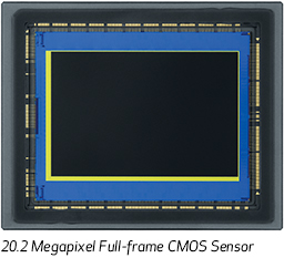
First of all, there’s the sensor, which includes a number of firsts for Canon. It’s a 20.2-million-pixel full frame CMOS sensor that’s the firm’s first to use on-chip analogue to digital conversion. Canon says that by shortening the signal pathways used when reading the signal off the sensor, this should result in lower noise, with the main benefit being increased dynamic range and cleaner shadows at low ISOs.
https://www.trustedreviews.com/reviews/canon-eos-1d-x-mark-ii
And one more thing:
These people modify 5DIVs, cooling the sensor for astronomical use.
Loading…
www.centralds.net
They say:
Recently the was a big development in Canon’s CMOS technology.
That is moved A/D converter into CMOS wafer (= On-chip ADC).
This jumped technology make possible to reduce dramatically Read Noise when the light signal is changed to electric signal. This is very helpful for low light photography such as astro imaging field and it make possible to separate the low signal from the background noise.
We can see the changed background noise pattern and can’t find any ‘banding noise’ the old issue of canon DSLRs.
Part of the conversion is to move the sensor, involving extending the cables from the sensor to the camera:
The CMOS cable delivers only digital signals. The lines are composed with pairs and the additional ground and shield has helped the stability of the circuit.
--
Ride easy, William.
Bob
Last edited:
Antisthenes
Forum Enthusiast
Logic doesn't seem to be your forte. There's no need for me to identify a candidate part — I've already told you that, as Canon likely buys millions of these chips, the part is quite likely a custom part specific for Canon, with specs not found anywhere in ADI's publcly available information.Some of the LDVS buffer chips come in BGA packages, and it possibly is not just a simple buffer. It's possibly a deserialiser, or other decoding function. AD makes all sorts of stuff. It doesn't match any of their AFEs.These LVDS transceivers are functionally simple devices, and come in small, in-line packages with a limited number of leads — around 8 to 20, they are just serial protocol conversion chips, after all — and their package looks completely different from the ADI chip found in the 5DIV.OK, lost track of which image you were referring to.The picture is actually of a 5D4 PCB...No, it isn't much more likely. By and large, I do like to do a bit of prior research before making a post.It's actually much more likely that Canon's image sensors —Practically every sensor in every camera you buy today has embedded column ADCs. Though they weren't the originators of the technology, Sony introduced it to the still camera market with the IMX021 in the Nikon D300 and Sony A700. Every Samsung sensor used it. Panasonic used the architecture from the GH2 onwards, Canon has used it from the 1D X II and most of their cameras now use it.Multiple A/Ds in parallel would definitely fix the A/D throughput problem. But embedded in the sensor? I'm not aware of camera sensors with embedded A/Ds. I can think of a lot of circuit problems that would create and not many advantages.Would not a bsi sensor with a higher number of embedded adcs offset that (at a higher sensor complexity/power cost)?I'm not a sensor expert but I do know about A/D converters. The higher the resolution (pixel count), the longer it takes for the A/D to convert all those analog pixel readings into their digital values, which affects shooting rate and power dissipation.
- It may also be that camera electronics can have difficulty to handle larger amount of data within limited power budget.
That's a 5Ds, not a 1D XII or 5D4. The 1D X II was, so far as I know the first Canon camera to have column ADCs and was widely reported to be so at the time.including the ones in the 1D X II and 5D4 — do not have on-chip ADCs and still use an external A/D conversion circuitry.
https://www.dpreview.com/forums/post/61749398
Indeed, AD, makers of all kinds of chip, including such things as LDVS transceivers:As to your "doing a bit of prior research", it seems to have escaped your attention that that PCB sports a chip manufactured by Analog Devices, Inc. — have you ever heard of that company ?
https://www.analog.com/en/parametricsearch/11462
which would typically be used to interface the output from a digital output sensors (which generally interface to LVDS) to a processor which doesn't have an LVDS interface (not so many do, built-in)
The ADI chip on the 5DIV PCB is a square — presumably BGA — chip that bears a striking physical resemblance to the ADI ADC chips customarily used in Canon's DSLRs.
Possibly the best way to find out what it is is to ask Roger Cicala, who does post here to look at the original, higher res version of the image and see whether the chip can be identified. Then we'll know for sure, and if I'm wrong, I will immediately accept it. Until then, your assumption that the chip must be an AFE doesn't hold much water. Can you even identify a candidate part?
The fact that Canon likely uses / licenses TI's ARM CPU and SoC-related intellectual property doesn't automatically mean that DIGICs are "off-the-shelf" chips. Given Canon's purchasing power and in-house design capabilities, it's quite possible that Canon actually design a significant part of the functionality of the ASIC they name "DIGIC", designing and adding to it various functionalities they might need for their cameras — e.g. I/O interfaces connected to the image sensor, memory cards, rear LCD, motor control etc.What do you think the DIGIC chips are? They are off-the-shelf application processor chips. Canon does not design them, Texas Instruments do. It's quite possible that for a quite esoteric interface, it was worth using an additional interface chip.Furthermore, you're implying that Canon's engineers were clever enough to add LVDS transceivers to their image sensor, but not to their latest DIGIC chip. Canon's engineers probbaly din't realize that their image sensors were going to be interfaced with their DIGIC chips. That sounds soooo plausible.
The resulting ASIC, incorporating Canon's and TI's IP, would then be manufactured at a foundry facility.
Here's a page that hints that Canon — which is a multi-billion high-technology company, after all — might well have in-house EDA tools and could be using VHDLs to design their own logic chips:
"[..] Ensuring Efficient Development of Large-Scale System LSI
Canon develops its own system LSIs, ..."
http://www.canon.com/technology/now/element/cp.html

It doesn't seem to occur to you that the AD80246 is not an "off-the-shelf" part. The fact that a Nikon D850 might contain an image sensor marked Sony, IMX-blah-blah doesn't mean that the D850 uses an "off-the-shelf" part, for example.It's possible, but there is the interesting fact that Canon's been happy to use off the shelf AD devices before,Given that Canon produces millions of DSLRs per year, it's quite likely that ADI is willing to produce custom ADC / analog front-end chips, whose reference numbers and specs won't be found on ADI's public product list.The other problem that you have, is if you believe the unidentified chip do be an AFE chip, that AD does not have one that handles 8 channels (which is why, for instance, the 5D III required four 2 channel chips)
https://www.analog.com/en/parametricsearch/11269
Like these four AFE chips from the 1DX II
AD80246 as also used in 1200D, Rebel T5, Canon 5D mark III, Canon 600D; Canon, Canon Rebel T3i; Canon 6D, Canon G1x.
and generally, one would expect a custom chip to be labelled 'Canon', if Canon retained the IP. If Canon didn't, it would go in the AD catalog.
There's no publicly available information for the AD80246 anywhere, which would tend to indicate that it's a custom development for one specific customer; the part is not publicized, and does not seem to be avaialble for purchase by customers other than Canon.
Huh ? Which "signal conditioning components" ? How could you tell ? Where have you seen a picture of an 1DXII sensor assembly, for example ?Also worth noting is the signal conditioning components right on the analog inputs, which seem to absent on the 1D XII. Notice also on the 1D X, they are on the back of the sensor assembly, not on the main PCB. I wonder why they changed that?
You seem not to be even aware that noise degrades DR, and that DR can thus be improved by reducing noise, including of the "read noise" variety...I wasn't talking about DR improvement, I was talking about the read noise characteristic. Different thing.There are other possible avenues for DR improvement.You can find it what you like. It's one of a number of indicators:The "reports" one reads on the Internet that the 1D X II has on-chip ADCs are just based on hearsay of uninformed speculation and unfounded assumptions — e.g. that one can tell (by the color ?) of the peripheral areas visible on a low-res picture of a sensor package that they are column ADCs. I find such assertions quite ridiculous, to be honest.
- the performance characterisation of the chip.
https://www.dpreview.com/forums/post/61785976
The electrical contact layout might as well have been influenced by the chip carrier's electrical and thermal characteristics, and tighter path length constraints between the silicon and the package's pins.Lessly oversize,Oversize top and bottom borders do not imply that they must be ADC structures, as such borders were already present in image sensors contemporaneous with the first generation Canon 1D X:- the layout of the chip interface, which is atypical of analog output chips, which typically have connections each end. Column ADC chips generally have power supplies distributed round all four sides, the reason being that if you don't, the column ADCs power consumption disrupts the rather delicate power supply arrangements to the pixel array
- the oversize top and bottom borders, required to accommodate the ADCs
- the visible ADC structures on the chip
https://cweb.canon.jp/eos/lineup/1dx/feature-highquality.html
The 1 DX chip is classic Canon, classic analog output, no complex power supply, connections concentrated at the ends, smaller borders top and bottom. The 1 DX II chip is a break in years of practice, with power supply distribution top and bottom, (to what, I wonder) what looks very like a digital IO on the left hand side. Actually quite similar to a Sony, but more tidily arranged.
and without the visible structures running along just where you'd expect the busses for a column ADC to run.
The 1DX has a 18MP sensor and a 12fps frame rate, and the sensor must thus have a 220 megapixels/sec output bandwidth.
The 1DX II has a 20MP sensor, but can also record 4K video at 60FPS. As a 4K frame contains about 8 million pixels, the 1DX II's sensor must have an output bandwidth of about 480 megapixels/sec. The much higher bandwidth requirement could have driven the chip designers to bring some electrical contacts closer to the middle of the chip, so that the output signals have a shorter path to travel.
"Very little resemblance" ? REALLY ?I'm not relying on any one thing, I produce a number of things together, and say that on the balance of probability Canon has produced column ADCs for this chip and the subsequent ones which behave similarly. See one duck, it might be a goose. See a couple, you get more sure they're ducks see five, you become pretty sure they're ducks.I, on the other hand, do not have to rely on chip border width,
Very little resemblance, in fact, apart from the AD logo, and AD makes a huge variety of chips. All you have is that there is a chip labelled AD in the path from sensor to processor. You have no idea what it is.and can simply point towards an ADI chip on the 5DIV's PCB that bears a striking resemblance with ADI's ADC chips found in other Canon cameras.
 vs. AD80246 ADC/AFE found on 5DIII's sensor board (right)")
Unidentified Analog Devices chip on 5DIV PCB (left) vs. AD80246 ADC/AFE found on 5DIII's sensor board (right)
Sorry to have been unclear. When I suggested that "blocking" patents might exist, I of course meant that Canon's competitors might be owning these patents, which would then "block" Canon from using some technology.Nothing indicates that they haven't. Why do you believe that they would be so laggardly when every other manufacturer and their dogs have column ADCsCanon have certainly been working on the technology, but nothing indicates that they turned it into mass production reality yet.- a number of Canon patents showing that they have been developing the technology.
It would be a bit silly to draw conclusions from one of those things, almost as silly as drawing a conclusion from a single unidentified AD chip on a PCB, but when you put them together, it's likely, in the absence of contrary evidence, that column ADCs is the correct diagnosis. After all, why would Canon not have produced column ADCs? Every other sensor manufacturer has.
So these are 'blocking patents' after the technology they're trying to block has been developed by someone else? That doesn't work. In any case, as I said, Canon has certainly produced demonstrator chips with column ADC, and they did it before the release of the 1D XII. Funny that.There might also be "blocking" patents — e.g. related to noise processing / digital CDS — already owned by competitors with much larger semiconductor / image sensor businesses, and who have done extensive R&D and actual manufacturing and patenting in the relevant analog and digital circuit technologies well before Canon.
Quoting people who are just parroting stuff they've read on some Internet forum or rumor site, and have no capability and willingness to actually verify by themselves whether, say, a signal carried by a flex cable is analog or digital adds absolutely zero credibility to your argument.The only argument that you have is a chip that could be many things. You think that you have discovered something big, but all you've discovered is a chip with AD on it. Identify what it is, I'd be more impressed.Your argument is thus basically of the level of people invoking "akums razor" [sic].
Also see https://www.dpreview.com/forums/post/61755597
And one other thing, when it was released, Canon said it had ADC on the sensor chip:
First of all, there’s the sensor, which includes a number of firsts for Canon. It’s a 20.2-million-pixel full frame CMOS sensor that’s the firm’s first to use on-chip analogue to digital conversion. Canon says that by shortening the signal pathways used when reading the signal off the sensor, this should result in lower noise, with the main benefit being increased dynamic range and cleaner shadows at low ISOs.
https://www.trustedreviews.com/reviews/canon-eos-1d-x-mark-ii
The modders at centralds.net, by the way, say "We guess that the CMOS cable delivers only digital signals."
Let me enlighten you: "guess" means, they do not actually know.
Last edited:
bobn2
Forum Pro
So far, you have one piece of evidence. An unknown chip form a manufacturer that makes many. That is the reason that you need to identify the chip to make your case, until you do that, the rest is bluster. I now have seven pieces of evidence, and could doubtless gather more. Non is but itself conclusive, but neither is your counter evidence, so where we stand now, my seven is beating your one. You have to find something else to make the case.Logic doesn't seem to be your forte. There's no need for me to identify a candidate part — I've already told you that, as Canon likely buys millions of these chips, the part is quite likely a custom part specific for Canon, with specs not found anywhere in ADI's publcly available information.Some of the LDVS buffer chips come in BGA packages, and it possibly is not just a simple buffer. It's possibly a deserialiser, or other decoding function. AD makes all sorts of stuff. It doesn't match any of their AFEs.These LVDS transceivers are functionally simple devices, and come in small, in-line packages with a limited number of leads — around 8 to 20, they are just serial protocol conversion chips, after all — and their package looks completely different from the ADI chip found in the 5DIV.OK, lost track of which image you were referring to.The picture is actually of a 5D4 PCB...No, it isn't much more likely. By and large, I do like to do a bit of prior research before making a post.It's actually much more likely that Canon's image sensors —Practically every sensor in every camera you buy today has embedded column ADCs. Though they weren't the originators of the technology, Sony introduced it to the still camera market with the IMX021 in the Nikon D300 and Sony A700. Every Samsung sensor used it. Panasonic used the architecture from the GH2 onwards, Canon has used it from the 1D X II and most of their cameras now use it.Multiple A/Ds in parallel would definitely fix the A/D throughput problem. But embedded in the sensor? I'm not aware of camera sensors with embedded A/Ds. I can think of a lot of circuit problems that would create and not many advantages.Would not a bsi sensor with a higher number of embedded adcs offset that (at a higher sensor complexity/power cost)?I'm not a sensor expert but I do know about A/D converters. The higher the resolution (pixel count), the longer it takes for the A/D to convert all those analog pixel readings into their digital values, which affects shooting rate and power dissipation.
- It may also be that camera electronics can have difficulty to handle larger amount of data within limited power budget.
That's a 5Ds, not a 1D XII or 5D4. The 1D X II was, so far as I know the first Canon camera to have column ADCs and was widely reported to be so at the time.including the ones in the 1D X II and 5D4 — do not have on-chip ADCs and still use an external A/D conversion circuitry.
https://www.dpreview.com/forums/post/61749398
Indeed, AD, makers of all kinds of chip, including such things as LDVS transceivers:As to your "doing a bit of prior research", it seems to have escaped your attention that that PCB sports a chip manufactured by Analog Devices, Inc. — have you ever heard of that company ?
https://www.analog.com/en/parametricsearch/11462
which would typically be used to interface the output from a digital output sensors (which generally interface to LVDS) to a processor which doesn't have an LVDS interface (not so many do, built-in)
The ADI chip on the 5DIV PCB is a square — presumably BGA — chip that bears a striking physical resemblance to the ADI ADC chips customarily used in Canon's DSLRs.
Possibly the best way to find out what it is is to ask Roger Cicala, who does post here to look at the original, higher res version of the image and see whether the chip can be identified. Then we'll know for sure, and if I'm wrong, I will immediately accept it. Until then, your assumption that the chip must be an AFE doesn't hold much water. Can you even identify a candidate part?
The fact that Canon likely uses / licenses TI's ARM CPU and SoC-related intellectual property doesn't automatically mean that DIGICs are "off-the-shelf" chips. Given Canon's purchasing power and in-house design capabilities, it's quite possible that Canon actually design a significant part of the functionality of the ASIC they name "DIGIC", designing and adding to it various functionalities they might need for their cameras — e.g. I/O interfaces connected to the image sensor, memory cards, rear LCD, motor control etc.What do you think the DIGIC chips are? They are off-the-shelf application processor chips. Canon does not design them, Texas Instruments do. It's quite possible that for a quite esoteric interface, it was worth using an additional interface chip.Furthermore, you're implying that Canon's engineers were clever enough to add LVDS transceivers to their image sensor, but not to their latest DIGIC chip. Canon's engineers probbaly din't realize that their image sensors were going to be interfaced with their DIGIC chips. That sounds soooo plausible.
The resulting ASIC, incorporating Canon's and TI's IP, would then be manufactured at a foundry facility.
Here's a page that hints that Canon — which is a multi-billion high-technology company, after all — might well have in-house EDA tools and could be using VHDLs to design their own logic chips:
"[..] Ensuring Efficient Development of Large-Scale System LSI
Canon develops its own system LSIs, ..."
http://www.canon.com/technology/now/element/cp.html
It doesn't seem to occur to you that the AD80246 is not an "off-the-shelf" part. The fact that a Nikon D850 might contain an image sensor marked Sony, IMX-blah-blah doesn't mean that the D850 uses an "off-the-shelf" part, for example.It's possible, but there is the interesting fact that Canon's been happy to use off the shelf AD devices before,Given that Canon produces millions of DSLRs per year, it's quite likely that ADI is willing to produce custom ADC / analog front-end chips, whose reference numbers and specs won't be found on ADI's public product list.The other problem that you have, is if you believe the unidentified chip do be an AFE chip, that AD does not have one that handles 8 channels (which is why, for instance, the 5D III required four 2 channel chips)
https://www.analog.com/en/parametricsearch/11269
Like these four AFE chips from the 1DX II
AD80246 as also used in 1200D, Rebel T5, Canon 5D mark III, Canon 600D; Canon, Canon Rebel T3i; Canon 6D, Canon G1x.
and generally, one would expect a custom chip to be labelled 'Canon', if Canon retained the IP. If Canon didn't, it would go in the AD catalog.
There's no publicly available information for the AD80246 anywhere, which would tend to indicate that it's a custom development for one specific customer; the part is not publicized, and does not seem to be avaialble for purchase by customers other than Canon.
Huh ? Which "signal conditioning components" ? How could you tell ? Where have you seen a picture of an 1DXII sensor assembly, for example ?Also worth noting is the signal conditioning components right on the analog inputs, which seem to absent on the 1D XII. Notice also on the 1D X, they are on the back of the sensor assembly, not on the main PCB. I wonder why they changed that?
You seem not to be even aware that noise degrades DR, and that DR can thus be improved by reducing noise, including of the "read noise" variety...I wasn't talking about DR improvement, I was talking about the read noise characteristic. Different thing.There are other possible avenues for DR improvement.You can find it what you like. It's one of a number of indicators:The "reports" one reads on the Internet that the 1D X II has on-chip ADCs are just based on hearsay of uninformed speculation and unfounded assumptions — e.g. that one can tell (by the color ?) of the peripheral areas visible on a low-res picture of a sensor package that they are column ADCs. I find such assertions quite ridiculous, to be honest.
- the performance characterisation of the chip.
https://www.dpreview.com/forums/post/61785976
The electrical contact layout might as well have been influenced by the chip carrier's electrical and thermal characteristics, and tighter path length constraints between the silicon and the package's pins.Lessly oversize,Oversize top and bottom borders do not imply that they must be ADC structures, as such borders were already present in image sensors contemporaneous with the first generation Canon 1D X:- the layout of the chip interface, which is atypical of analog output chips, which typically have connections each end. Column ADC chips generally have power supplies distributed round all four sides, the reason being that if you don't, the column ADCs power consumption disrupts the rather delicate power supply arrangements to the pixel array
- the oversize top and bottom borders, required to accommodate the ADCs
- the visible ADC structures on the chip
https://cweb.canon.jp/eos/lineup/1dx/feature-highquality.html
The 1 DX chip is classic Canon, classic analog output, no complex power supply, connections concentrated at the ends, smaller borders top and bottom. The 1 DX II chip is a break in years of practice, with power supply distribution top and bottom, (to what, I wonder) what looks very like a digital IO on the left hand side. Actually quite similar to a Sony, but more tidily arranged.
and without the visible structures running along just where you'd expect the busses for a column ADC to run.
The 1DX has a 18MP sensor and a 12fps frame rate, and the sensor must thus have a 220 megapixels/sec output bandwidth.
The 1DX II has a 20MP sensor, but can also record 4K video at 60FPS. As a 4K frame contains about 8 million pixels, the 1DX II's sensor must have an output bandwidth of about 480 megapixels/sec. The much higher bandwidth requirement could have driven the chip designers to bring some electrical contacts closer to the middle of the chip, so that the output signals have a shorter path to travel.
"Very little resemblance" ? REALLY ?I'm not relying on any one thing, I produce a number of things together, and say that on the balance of probability Canon has produced column ADCs for this chip and the subsequent ones which behave similarly. See one duck, it might be a goose. See a couple, you get more sure they're ducks see five, you become pretty sure they're ducks.I, on the other hand, do not have to rely on chip border width,
Very little resemblance, in fact, apart from the AD logo, and AD makes a huge variety of chips. All you have is that there is a chip labelled AD in the path from sensor to processor. You have no idea what it is.and can simply point towards an ADI chip on the 5DIV's PCB that bears a striking resemblance with ADI's ADC chips found in other Canon cameras.
Unidentified Analog Devices chip on 5DIV PCB (left) vs. AD80246 ADC/AFE found on 5DIII's sensor board (right)
Sorry to have been unclear. When I suggested that "blocking" patents might exist, I of course meant that Canon's competitors might be owning these patents, which would then "block" Canon from using some technology.Nothing indicates that they haven't. Why do you believe that they would be so laggardly when every other manufacturer and their dogs have column ADCsCanon have certainly been working on the technology, but nothing indicates that they turned it into mass production reality yet.- a number of Canon patents showing that they have been developing the technology.
It would be a bit silly to draw conclusions from one of those things, almost as silly as drawing a conclusion from a single unidentified AD chip on a PCB, but when you put them together, it's likely, in the absence of contrary evidence, that column ADCs is the correct diagnosis. After all, why would Canon not have produced column ADCs? Every other sensor manufacturer has.
So these are 'blocking patents' after the technology they're trying to block has been developed by someone else? That doesn't work. In any case, as I said, Canon has certainly produced demonstrator chips with column ADC, and they did it before the release of the 1D XII. Funny that.There might also be "blocking" patents — e.g. related to noise processing / digital CDS — already owned by competitors with much larger semiconductor / image sensor businesses, and who have done extensive R&D and actual manufacturing and patenting in the relevant analog and digital circuit technologies well before Canon.
Quoting people who are just parroting stuff they've read on some Internet forum or rumor site, and have no capability and willingness to actually verify by themselves whether, say, a signal carried by a flex cable is analog or digital adds absolutely zero credibility to your argument.The only argument that you have is a chip that could be many things. You think that you have discovered something big, but all you've discovered is a chip with AD on it. Identify what it is, I'd be more impressed.Your argument is thus basically of the level of people invoking "akums razor" [sic].
Also see https://www.dpreview.com/forums/post/61755597
And one other thing, when it was released, Canon said it had ADC on the sensor chip:
First of all, there’s the sensor, which includes a number of firsts for Canon. It’s a 20.2-million-pixel full frame CMOS sensor that’s the firm’s first to use on-chip analogue to digital conversion. Canon says that by shortening the signal pathways used when reading the signal off the sensor, this should result in lower noise, with the main benefit being increased dynamic range and cleaner shadows at low ISOs.
https://www.trustedreviews.com/reviews/canon-eos-1d-x-mark-ii
The modders at centralds.net, by the way, say "We guess that the CMOS cable delivers only digital signals."
Let me enlighten you: "guess" means, they do not actually know.
--
Ride easy, William.
Bob
Antisthenes
Forum Enthusiast
Given the intelelctual standards you've demonstrated when qualifying something as "evidence", I pity the person who'll have to stand trial before a jury containing the likes of you...So far, you have one piece of evidence. An unknown chip form a manufacturer that makes many. That is the reason that you need to identify the chip to make your case, until you do that, the rest is bluster. I now have seven pieces of evidence, and could doubtless gather more. Non is but itself conclusive, but neither is your counter evidence, so where we stand now, my seven is beating your one. You have to find something else to make the case.Logic doesn't seem to be your forte. There's no need for me to identify a candidate part — I've already told you that, as Canon likely buys millions of these chips, the part is quite likely a custom part specific for Canon, with specs not found anywhere in ADI's publcly available information.Some of the LDVS buffer chips come in BGA packages, and it possibly is not just a simple buffer. It's possibly a deserialiser, or other decoding function. AD makes all sorts of stuff. It doesn't match any of their AFEs.These LVDS transceivers are functionally simple devices, and come in small, in-line packages with a limited number of leads — around 8 to 20, they are just serial protocol conversion chips, after all — and their package looks completely different from the ADI chip found in the 5DIV.OK, lost track of which image you were referring to.The picture is actually of a 5D4 PCB...No, it isn't much more likely. By and large, I do like to do a bit of prior research before making a post.It's actually much more likely that Canon's image sensors —Practically every sensor in every camera you buy today has embedded column ADCs. Though they weren't the originators of the technology, Sony introduced it to the still camera market with the IMX021 in the Nikon D300 and Sony A700. Every Samsung sensor used it. Panasonic used the architecture from the GH2 onwards, Canon has used it from the 1D X II and most of their cameras now use it.Multiple A/Ds in parallel would definitely fix the A/D throughput problem. But embedded in the sensor? I'm not aware of camera sensors with embedded A/Ds. I can think of a lot of circuit problems that would create and not many advantages.Would not a bsi sensor with a higher number of embedded adcs offset that (at a higher sensor complexity/power cost)?I'm not a sensor expert but I do know about A/D converters. The higher the resolution (pixel count), the longer it takes for the A/D to convert all those analog pixel readings into their digital values, which affects shooting rate and power dissipation.
- It may also be that camera electronics can have difficulty to handle larger amount of data within limited power budget.
That's a 5Ds, not a 1D XII or 5D4. The 1D X II was, so far as I know the first Canon camera to have column ADCs and was widely reported to be so at the time.including the ones in the 1D X II and 5D4 — do not have on-chip ADCs and still use an external A/D conversion circuitry.
https://www.dpreview.com/forums/post/61749398
Indeed, AD, makers of all kinds of chip, including such things as LDVS transceivers:As to your "doing a bit of prior research", it seems to have escaped your attention that that PCB sports a chip manufactured by Analog Devices, Inc. — have you ever heard of that company ?
https://www.analog.com/en/parametricsearch/11462
which would typically be used to interface the output from a digital output sensors (which generally interface to LVDS) to a processor which doesn't have an LVDS interface (not so many do, built-in)
The ADI chip on the 5DIV PCB is a square — presumably BGA — chip that bears a striking physical resemblance to the ADI ADC chips customarily used in Canon's DSLRs.
Possibly the best way to find out what it is is to ask Roger Cicala, who does post here to look at the original, higher res version of the image and see whether the chip can be identified. Then we'll know for sure, and if I'm wrong, I will immediately accept it. Until then, your assumption that the chip must be an AFE doesn't hold much water. Can you even identify a candidate part?
The fact that Canon likely uses / licenses TI's ARM CPU and SoC-related intellectual property doesn't automatically mean that DIGICs are "off-the-shelf" chips. Given Canon's purchasing power and in-house design capabilities, it's quite possible that Canon actually design a significant part of the functionality of the ASIC they name "DIGIC", designing and adding to it various functionalities they might need for their cameras — e.g. I/O interfaces connected to the image sensor, memory cards, rear LCD, motor control etc.What do you think the DIGIC chips are? They are off-the-shelf application processor chips. Canon does not design them, Texas Instruments do. It's quite possible that for a quite esoteric interface, it was worth using an additional interface chip.Furthermore, you're implying that Canon's engineers were clever enough to add LVDS transceivers to their image sensor, but not to their latest DIGIC chip. Canon's engineers probbaly din't realize that their image sensors were going to be interfaced with their DIGIC chips. That sounds soooo plausible.
The resulting ASIC, incorporating Canon's and TI's IP, would then be manufactured at a foundry facility.
Here's a page that hints that Canon — which is a multi-billion high-technology company, after all — might well have in-house EDA tools and could be using VHDLs to design their own logic chips:
"[..] Ensuring Efficient Development of Large-Scale System LSI
Canon develops its own system LSIs, ..."
http://www.canon.com/technology/now/element/cp.html
It doesn't seem to occur to you that the AD80246 is not an "off-the-shelf" part. The fact that a Nikon D850 might contain an image sensor marked Sony, IMX-blah-blah doesn't mean that the D850 uses an "off-the-shelf" part, for example.It's possible, but there is the interesting fact that Canon's been happy to use off the shelf AD devices before,Given that Canon produces millions of DSLRs per year, it's quite likely that ADI is willing to produce custom ADC / analog front-end chips, whose reference numbers and specs won't be found on ADI's public product list.The other problem that you have, is if you believe the unidentified chip do be an AFE chip, that AD does not have one that handles 8 channels (which is why, for instance, the 5D III required four 2 channel chips)
https://www.analog.com/en/parametricsearch/11269
Like these four AFE chips from the 1DX II
AD80246 as also used in 1200D, Rebel T5, Canon 5D mark III, Canon 600D; Canon, Canon Rebel T3i; Canon 6D, Canon G1x.
and generally, one would expect a custom chip to be labelled 'Canon', if Canon retained the IP. If Canon didn't, it would go in the AD catalog.
There's no publicly available information for the AD80246 anywhere, which would tend to indicate that it's a custom development for one specific customer; the part is not publicized, and does not seem to be avaialble for purchase by customers other than Canon.
Huh ? Which "signal conditioning components" ? How could you tell ? Where have you seen a picture of an 1DXII sensor assembly, for example ?Also worth noting is the signal conditioning components right on the analog inputs, which seem to absent on the 1D XII. Notice also on the 1D X, they are on the back of the sensor assembly, not on the main PCB. I wonder why they changed that?
You seem not to be even aware that noise degrades DR, and that DR can thus be improved by reducing noise, including of the "read noise" variety...I wasn't talking about DR improvement, I was talking about the read noise characteristic. Different thing.There are other possible avenues for DR improvement.You can find it what you like. It's one of a number of indicators:The "reports" one reads on the Internet that the 1D X II has on-chip ADCs are just based on hearsay of uninformed speculation and unfounded assumptions — e.g. that one can tell (by the color ?) of the peripheral areas visible on a low-res picture of a sensor package that they are column ADCs. I find such assertions quite ridiculous, to be honest.
- the performance characterisation of the chip.
https://www.dpreview.com/forums/post/61785976
The electrical contact layout might as well have been influenced by the chip carrier's electrical and thermal characteristics, and tighter path length constraints between the silicon and the package's pins.Lessly oversize,Oversize top and bottom borders do not imply that they must be ADC structures, as such borders were already present in image sensors contemporaneous with the first generation Canon 1D X:- the layout of the chip interface, which is atypical of analog output chips, which typically have connections each end. Column ADC chips generally have power supplies distributed round all four sides, the reason being that if you don't, the column ADCs power consumption disrupts the rather delicate power supply arrangements to the pixel array
- the oversize top and bottom borders, required to accommodate the ADCs
- the visible ADC structures on the chip
https://cweb.canon.jp/eos/lineup/1dx/feature-highquality.html
The 1 DX chip is classic Canon, classic analog output, no complex power supply, connections concentrated at the ends, smaller borders top and bottom. The 1 DX II chip is a break in years of practice, with power supply distribution top and bottom, (to what, I wonder) what looks very like a digital IO on the left hand side. Actually quite similar to a Sony, but more tidily arranged.
and without the visible structures running along just where you'd expect the busses for a column ADC to run.
The 1DX has a 18MP sensor and a 12fps frame rate, and the sensor must thus have a 220 megapixels/sec output bandwidth.
The 1DX II has a 20MP sensor, but can also record 4K video at 60FPS. As a 4K frame contains about 8 million pixels, the 1DX II's sensor must have an output bandwidth of about 480 megapixels/sec. The much higher bandwidth requirement could have driven the chip designers to bring some electrical contacts closer to the middle of the chip, so that the output signals have a shorter path to travel.
"Very little resemblance" ? REALLY ?I'm not relying on any one thing, I produce a number of things together, and say that on the balance of probability Canon has produced column ADCs for this chip and the subsequent ones which behave similarly. See one duck, it might be a goose. See a couple, you get more sure they're ducks see five, you become pretty sure they're ducks.I, on the other hand, do not have to rely on chip border width,
Very little resemblance, in fact, apart from the AD logo, and AD makes a huge variety of chips. All you have is that there is a chip labelled AD in the path from sensor to processor. You have no idea what it is.and can simply point towards an ADI chip on the 5DIV's PCB that bears a striking resemblance with ADI's ADC chips found in other Canon cameras.
Unidentified Analog Devices chip on 5DIV PCB (left) vs. AD80246 ADC/AFE found on 5DIII's sensor board (right)
Sorry to have been unclear. When I suggested that "blocking" patents might exist, I of course meant that Canon's competitors might be owning these patents, which would then "block" Canon from using some technology.Nothing indicates that they haven't. Why do you believe that they would be so laggardly when every other manufacturer and their dogs have column ADCsCanon have certainly been working on the technology, but nothing indicates that they turned it into mass production reality yet.- a number of Canon patents showing that they have been developing the technology.
It would be a bit silly to draw conclusions from one of those things, almost as silly as drawing a conclusion from a single unidentified AD chip on a PCB, but when you put them together, it's likely, in the absence of contrary evidence, that column ADCs is the correct diagnosis. After all, why would Canon not have produced column ADCs? Every other sensor manufacturer has.
So these are 'blocking patents' after the technology they're trying to block has been developed by someone else? That doesn't work. In any case, as I said, Canon has certainly produced demonstrator chips with column ADC, and they did it before the release of the 1D XII. Funny that.There might also be "blocking" patents — e.g. related to noise processing / digital CDS — already owned by competitors with much larger semiconductor / image sensor businesses, and who have done extensive R&D and actual manufacturing and patenting in the relevant analog and digital circuit technologies well before Canon.
Quoting people who are just parroting stuff they've read on some Internet forum or rumor site, and have no capability and willingness to actually verify by themselves whether, say, a signal carried by a flex cable is analog or digital adds absolutely zero credibility to your argument.The only argument that you have is a chip that could be many things. You think that you have discovered something big, but all you've discovered is a chip with AD on it. Identify what it is, I'd be more impressed.Your argument is thus basically of the level of people invoking "akums razor" [sic].
Also see https://www.dpreview.com/forums/post/61755597
And one other thing, when it was released, Canon said it had ADC on the sensor chip:
First of all, there’s the sensor, which includes a number of firsts for Canon. It’s a 20.2-million-pixel full frame CMOS sensor that’s the firm’s first to use on-chip analogue to digital conversion. Canon says that by shortening the signal pathways used when reading the signal off the sensor, this should result in lower noise, with the main benefit being increased dynamic range and cleaner shadows at low ISOs.
https://www.trustedreviews.com/reviews/canon-eos-1d-x-mark-ii
The modders at centralds.net, by the way, say "We guess that the CMOS cable delivers only digital signals."
Let me enlighten you: "guess" means, they do not actually know.
Last edited:
bobn2
Forum Pro
So, you're signalling the end of a rational discussion, and on to the ad-hominem stuff in the absence of anything else to support your case. Time, I think, to call a halt.Given the intelelctual standards you've demonstrated when qualifying something as "evidence", I pity the person who'll have to stand trial before a jury containing the likes of you...So far, you have one piece of evidence. An unknown chip form a manufacturer that makes many. That is the reason that you need to identify the chip to make your case, until you do that, the rest is bluster. I now have seven pieces of evidence, and could doubtless gather more. Non is but itself conclusive, but neither is your counter evidence, so where we stand now, my seven is beating your one. You have to find something else to make the case.Logic doesn't seem to be your forte. There's no need for me to identify a candidate part — I've already told you that, as Canon likely buys millions of these chips, the part is quite likely a custom part specific for Canon, with specs not found anywhere in ADI's publcly available information.Some of the LDVS buffer chips come in BGA packages, and it possibly is not just a simple buffer. It's possibly a deserialiser, or other decoding function. AD makes all sorts of stuff. It doesn't match any of their AFEs.These LVDS transceivers are functionally simple devices, and come in small, in-line packages with a limited number of leads — around 8 to 20, they are just serial protocol conversion chips, after all — and their package looks completely different from the ADI chip found in the 5DIV.OK, lost track of which image you were referring to.The picture is actually of a 5D4 PCB...No, it isn't much more likely. By and large, I do like to do a bit of prior research before making a post.It's actually much more likely that Canon's image sensors —Practically every sensor in every camera you buy today has embedded column ADCs. Though they weren't the originators of the technology, Sony introduced it to the still camera market with the IMX021 in the Nikon D300 and Sony A700. Every Samsung sensor used it. Panasonic used the architecture from the GH2 onwards, Canon has used it from the 1D X II and most of their cameras now use it.Multiple A/Ds in parallel would definitely fix the A/D throughput problem. But embedded in the sensor? I'm not aware of camera sensors with embedded A/Ds. I can think of a lot of circuit problems that would create and not many advantages.Would not a bsi sensor with a higher number of embedded adcs offset that (at a higher sensor complexity/power cost)?I'm not a sensor expert but I do know about A/D converters. The higher the resolution (pixel count), the longer it takes for the A/D to convert all those analog pixel readings into their digital values, which affects shooting rate and power dissipation.
- It may also be that camera electronics can have difficulty to handle larger amount of data within limited power budget.
That's a 5Ds, not a 1D XII or 5D4. The 1D X II was, so far as I know the first Canon camera to have column ADCs and was widely reported to be so at the time.including the ones in the 1D X II and 5D4 — do not have on-chip ADCs and still use an external A/D conversion circuitry.
https://www.dpreview.com/forums/post/61749398
Indeed, AD, makers of all kinds of chip, including such things as LDVS transceivers:As to your "doing a bit of prior research", it seems to have escaped your attention that that PCB sports a chip manufactured by Analog Devices, Inc. — have you ever heard of that company ?
https://www.analog.com/en/parametricsearch/11462
which would typically be used to interface the output from a digital output sensors (which generally interface to LVDS) to a processor which doesn't have an LVDS interface (not so many do, built-in)
The ADI chip on the 5DIV PCB is a square — presumably BGA — chip that bears a striking physical resemblance to the ADI ADC chips customarily used in Canon's DSLRs.
Possibly the best way to find out what it is is to ask Roger Cicala, who does post here to look at the original, higher res version of the image and see whether the chip can be identified. Then we'll know for sure, and if I'm wrong, I will immediately accept it. Until then, your assumption that the chip must be an AFE doesn't hold much water. Can you even identify a candidate part?
The fact that Canon likely uses / licenses TI's ARM CPU and SoC-related intellectual property doesn't automatically mean that DIGICs are "off-the-shelf" chips. Given Canon's purchasing power and in-house design capabilities, it's quite possible that Canon actually design a significant part of the functionality of the ASIC they name "DIGIC", designing and adding to it various functionalities they might need for their cameras — e.g. I/O interfaces connected to the image sensor, memory cards, rear LCD, motor control etc.What do you think the DIGIC chips are? They are off-the-shelf application processor chips. Canon does not design them, Texas Instruments do. It's quite possible that for a quite esoteric interface, it was worth using an additional interface chip.Furthermore, you're implying that Canon's engineers were clever enough to add LVDS transceivers to their image sensor, but not to their latest DIGIC chip. Canon's engineers probbaly din't realize that their image sensors were going to be interfaced with their DIGIC chips. That sounds soooo plausible.
The resulting ASIC, incorporating Canon's and TI's IP, would then be manufactured at a foundry facility.
Here's a page that hints that Canon — which is a multi-billion high-technology company, after all — might well have in-house EDA tools and could be using VHDLs to design their own logic chips:
"[..] Ensuring Efficient Development of Large-Scale System LSI
Canon develops its own system LSIs, ..."
http://www.canon.com/technology/now/element/cp.html
It doesn't seem to occur to you that the AD80246 is not an "off-the-shelf" part. The fact that a Nikon D850 might contain an image sensor marked Sony, IMX-blah-blah doesn't mean that the D850 uses an "off-the-shelf" part, for example.It's possible, but there is the interesting fact that Canon's been happy to use off the shelf AD devices before,Given that Canon produces millions of DSLRs per year, it's quite likely that ADI is willing to produce custom ADC / analog front-end chips, whose reference numbers and specs won't be found on ADI's public product list.The other problem that you have, is if you believe the unidentified chip do be an AFE chip, that AD does not have one that handles 8 channels (which is why, for instance, the 5D III required four 2 channel chips)
https://www.analog.com/en/parametricsearch/11269
Like these four AFE chips from the 1DX II
AD80246 as also used in 1200D, Rebel T5, Canon 5D mark III, Canon 600D; Canon, Canon Rebel T3i; Canon 6D, Canon G1x.
and generally, one would expect a custom chip to be labelled 'Canon', if Canon retained the IP. If Canon didn't, it would go in the AD catalog.
There's no publicly available information for the AD80246 anywhere, which would tend to indicate that it's a custom development for one specific customer; the part is not publicized, and does not seem to be avaialble for purchase by customers other than Canon.
Huh ? Which "signal conditioning components" ? How could you tell ? Where have you seen a picture of an 1DXII sensor assembly, for example ?Also worth noting is the signal conditioning components right on the analog inputs, which seem to absent on the 1D XII. Notice also on the 1D X, they are on the back of the sensor assembly, not on the main PCB. I wonder why they changed that?
You seem not to be even aware that noise degrades DR, and that DR can thus be improved by reducing noise, including of the "read noise" variety...I wasn't talking about DR improvement, I was talking about the read noise characteristic. Different thing.There are other possible avenues for DR improvement.You can find it what you like. It's one of a number of indicators:The "reports" one reads on the Internet that the 1D X II has on-chip ADCs are just based on hearsay of uninformed speculation and unfounded assumptions — e.g. that one can tell (by the color ?) of the peripheral areas visible on a low-res picture of a sensor package that they are column ADCs. I find such assertions quite ridiculous, to be honest.
- the performance characterisation of the chip.
https://www.dpreview.com/forums/post/61785976
The electrical contact layout might as well have been influenced by the chip carrier's electrical and thermal characteristics, and tighter path length constraints between the silicon and the package's pins.Lessly oversize,Oversize top and bottom borders do not imply that they must be ADC structures, as such borders were already present in image sensors contemporaneous with the first generation Canon 1D X:- the layout of the chip interface, which is atypical of analog output chips, which typically have connections each end. Column ADC chips generally have power supplies distributed round all four sides, the reason being that if you don't, the column ADCs power consumption disrupts the rather delicate power supply arrangements to the pixel array
- the oversize top and bottom borders, required to accommodate the ADCs
- the visible ADC structures on the chip
https://cweb.canon.jp/eos/lineup/1dx/feature-highquality.html
The 1 DX chip is classic Canon, classic analog output, no complex power supply, connections concentrated at the ends, smaller borders top and bottom. The 1 DX II chip is a break in years of practice, with power supply distribution top and bottom, (to what, I wonder) what looks very like a digital IO on the left hand side. Actually quite similar to a Sony, but more tidily arranged.
and without the visible structures running along just where you'd expect the busses for a column ADC to run.
The 1DX has a 18MP sensor and a 12fps frame rate, and the sensor must thus have a 220 megapixels/sec output bandwidth.
The 1DX II has a 20MP sensor, but can also record 4K video at 60FPS. As a 4K frame contains about 8 million pixels, the 1DX II's sensor must have an output bandwidth of about 480 megapixels/sec. The much higher bandwidth requirement could have driven the chip designers to bring some electrical contacts closer to the middle of the chip, so that the output signals have a shorter path to travel.
"Very little resemblance" ? REALLY ?I'm not relying on any one thing, I produce a number of things together, and say that on the balance of probability Canon has produced column ADCs for this chip and the subsequent ones which behave similarly. See one duck, it might be a goose. See a couple, you get more sure they're ducks see five, you become pretty sure they're ducks.I, on the other hand, do not have to rely on chip border width,
Very little resemblance, in fact, apart from the AD logo, and AD makes a huge variety of chips. All you have is that there is a chip labelled AD in the path from sensor to processor. You have no idea what it is.and can simply point towards an ADI chip on the 5DIV's PCB that bears a striking resemblance with ADI's ADC chips found in other Canon cameras.
Unidentified Analog Devices chip on 5DIV PCB (left) vs. AD80246 ADC/AFE found on 5DIII's sensor board (right)
Sorry to have been unclear. When I suggested that "blocking" patents might exist, I of course meant that Canon's competitors might be owning these patents, which would then "block" Canon from using some technology.Nothing indicates that they haven't. Why do you believe that they would be so laggardly when every other manufacturer and their dogs have column ADCsCanon have certainly been working on the technology, but nothing indicates that they turned it into mass production reality yet.- a number of Canon patents showing that they have been developing the technology.
It would be a bit silly to draw conclusions from one of those things, almost as silly as drawing a conclusion from a single unidentified AD chip on a PCB, but when you put them together, it's likely, in the absence of contrary evidence, that column ADCs is the correct diagnosis. After all, why would Canon not have produced column ADCs? Every other sensor manufacturer has.
So these are 'blocking patents' after the technology they're trying to block has been developed by someone else? That doesn't work. In any case, as I said, Canon has certainly produced demonstrator chips with column ADC, and they did it before the release of the 1D XII. Funny that.There might also be "blocking" patents — e.g. related to noise processing / digital CDS — already owned by competitors with much larger semiconductor / image sensor businesses, and who have done extensive R&D and actual manufacturing and patenting in the relevant analog and digital circuit technologies well before Canon.
Quoting people who are just parroting stuff they've read on some Internet forum or rumor site, and have no capability and willingness to actually verify by themselves whether, say, a signal carried by a flex cable is analog or digital adds absolutely zero credibility to your argument.The only argument that you have is a chip that could be many things. You think that you have discovered something big, but all you've discovered is a chip with AD on it. Identify what it is, I'd be more impressed.Your argument is thus basically of the level of people invoking "akums razor" [sic].
Also see https://www.dpreview.com/forums/post/61755597
And one other thing, when it was released, Canon said it had ADC on the sensor chip:
First of all, there’s the sensor, which includes a number of firsts for Canon. It’s a 20.2-million-pixel full frame CMOS sensor that’s the firm’s first to use on-chip analogue to digital conversion. Canon says that by shortening the signal pathways used when reading the signal off the sensor, this should result in lower noise, with the main benefit being increased dynamic range and cleaner shadows at low ISOs.
https://www.trustedreviews.com/reviews/canon-eos-1d-x-mark-ii
The modders at centralds.net, by the way, say "We guess that the CMOS cable delivers only digital signals."
Let me enlighten you: "guess" means, they do not actually know.
--
Ride easy, William.
Bob
Antisthenes
Forum Enthusiast
As soon as you start to qualify as "evidence" something that isn't — e.g. postulating that an oversize border on the sensor chip is necessarily an ADC circuitry, or citing random pronouncements found on the Internet, or postulating unplausible roles like LVDS conversion for a particular chip, etc. — then, the discussion belongs more to the domain of fantasy than rationality.So, you're signalling the end of a rational discussion, and on to the ad-hominem stuff in the absence of anything else to support your case. Time, I think, to call a halt.Given the intelelctual standards you've demonstrated when qualifying something as "evidence", I pity the person who'll have to stand trial before a jury containing the likes of you...So far, you have one piece of evidence. An unknown chip form a manufacturer that makes many. That is the reason that you need to identify the chip to make your case, until you do that, the rest is bluster. I now have seven pieces of evidence, and could doubtless gather more. Non is but itself conclusive, but neither is your counter evidence, so where we stand now, my seven is beating your one. You have to find something else to make the case.Logic doesn't seem to be your forte. There's no need for me to identify a candidate part — I've already told you that, as Canon likely buys millions of these chips, the part is quite likely a custom part specific for Canon, with specs not found anywhere in ADI's publcly available information.Some of the LDVS buffer chips come in BGA packages, and it possibly is not just a simple buffer. It's possibly a deserialiser, or other decoding function. AD makes all sorts of stuff. It doesn't match any of their AFEs.These LVDS transceivers are functionally simple devices, and come in small, in-line packages with a limited number of leads — around 8 to 20, they are just serial protocol conversion chips, after all — and their package looks completely different from the ADI chip found in the 5DIV.OK, lost track of which image you were referring to.The picture is actually of a 5D4 PCB...No, it isn't much more likely. By and large, I do like to do a bit of prior research before making a post.It's actually much more likely that Canon's image sensors —Practically every sensor in every camera you buy today has embedded column ADCs. Though they weren't the originators of the technology, Sony introduced it to the still camera market with the IMX021 in the Nikon D300 and Sony A700. Every Samsung sensor used it. Panasonic used the architecture from the GH2 onwards, Canon has used it from the 1D X II and most of their cameras now use it.Multiple A/Ds in parallel would definitely fix the A/D throughput problem. But embedded in the sensor? I'm not aware of camera sensors with embedded A/Ds. I can think of a lot of circuit problems that would create and not many advantages.Would not a bsi sensor with a higher number of embedded adcs offset that (at a higher sensor complexity/power cost)?I'm not a sensor expert but I do know about A/D converters. The higher the resolution (pixel count), the longer it takes for the A/D to convert all those analog pixel readings into their digital values, which affects shooting rate and power dissipation.
- It may also be that camera electronics can have difficulty to handle larger amount of data within limited power budget.
That's a 5Ds, not a 1D XII or 5D4. The 1D X II was, so far as I know the first Canon camera to have column ADCs and was widely reported to be so at the time.including the ones in the 1D X II and 5D4 — do not have on-chip ADCs and still use an external A/D conversion circuitry.
https://www.dpreview.com/forums/post/61749398
Indeed, AD, makers of all kinds of chip, including such things as LDVS transceivers:As to your "doing a bit of prior research", it seems to have escaped your attention that that PCB sports a chip manufactured by Analog Devices, Inc. — have you ever heard of that company ?
https://www.analog.com/en/parametricsearch/11462
which would typically be used to interface the output from a digital output sensors (which generally interface to LVDS) to a processor which doesn't have an LVDS interface (not so many do, built-in)
The ADI chip on the 5DIV PCB is a square — presumably BGA — chip that bears a striking physical resemblance to the ADI ADC chips customarily used in Canon's DSLRs.
Possibly the best way to find out what it is is to ask Roger Cicala, who does post here to look at the original, higher res version of the image and see whether the chip can be identified. Then we'll know for sure, and if I'm wrong, I will immediately accept it. Until then, your assumption that the chip must be an AFE doesn't hold much water. Can you even identify a candidate part?
The fact that Canon likely uses / licenses TI's ARM CPU and SoC-related intellectual property doesn't automatically mean that DIGICs are "off-the-shelf" chips. Given Canon's purchasing power and in-house design capabilities, it's quite possible that Canon actually design a significant part of the functionality of the ASIC they name "DIGIC", designing and adding to it various functionalities they might need for their cameras — e.g. I/O interfaces connected to the image sensor, memory cards, rear LCD, motor control etc.What do you think the DIGIC chips are? They are off-the-shelf application processor chips. Canon does not design them, Texas Instruments do. It's quite possible that for a quite esoteric interface, it was worth using an additional interface chip.Furthermore, you're implying that Canon's engineers were clever enough to add LVDS transceivers to their image sensor, but not to their latest DIGIC chip. Canon's engineers probbaly din't realize that their image sensors were going to be interfaced with their DIGIC chips. That sounds soooo plausible.
The resulting ASIC, incorporating Canon's and TI's IP, would then be manufactured at a foundry facility.
Here's a page that hints that Canon — which is a multi-billion high-technology company, after all — might well have in-house EDA tools and could be using VHDLs to design their own logic chips:
"[..] Ensuring Efficient Development of Large-Scale System LSI
Canon develops its own system LSIs, ..."
http://www.canon.com/technology/now/element/cp.html
It doesn't seem to occur to you that the AD80246 is not an "off-the-shelf" part. The fact that a Nikon D850 might contain an image sensor marked Sony, IMX-blah-blah doesn't mean that the D850 uses an "off-the-shelf" part, for example.It's possible, but there is the interesting fact that Canon's been happy to use off the shelf AD devices before,Given that Canon produces millions of DSLRs per year, it's quite likely that ADI is willing to produce custom ADC / analog front-end chips, whose reference numbers and specs won't be found on ADI's public product list.The other problem that you have, is if you believe the unidentified chip do be an AFE chip, that AD does not have one that handles 8 channels (which is why, for instance, the 5D III required four 2 channel chips)
https://www.analog.com/en/parametricsearch/11269
Like these four AFE chips from the 1DX II
AD80246 as also used in 1200D, Rebel T5, Canon 5D mark III, Canon 600D; Canon, Canon Rebel T3i; Canon 6D, Canon G1x.
and generally, one would expect a custom chip to be labelled 'Canon', if Canon retained the IP. If Canon didn't, it would go in the AD catalog.
There's no publicly available information for the AD80246 anywhere, which would tend to indicate that it's a custom development for one specific customer; the part is not publicized, and does not seem to be avaialble for purchase by customers other than Canon.
Huh ? Which "signal conditioning components" ? How could you tell ? Where have you seen a picture of an 1DXII sensor assembly, for example ?Also worth noting is the signal conditioning components right on the analog inputs, which seem to absent on the 1D XII. Notice also on the 1D X, they are on the back of the sensor assembly, not on the main PCB. I wonder why they changed that?
You seem not to be even aware that noise degrades DR, and that DR can thus be improved by reducing noise, including of the "read noise" variety...I wasn't talking about DR improvement, I was talking about the read noise characteristic. Different thing.There are other possible avenues for DR improvement.You can find it what you like. It's one of a number of indicators:The "reports" one reads on the Internet that the 1D X II has on-chip ADCs are just based on hearsay of uninformed speculation and unfounded assumptions — e.g. that one can tell (by the color ?) of the peripheral areas visible on a low-res picture of a sensor package that they are column ADCs. I find such assertions quite ridiculous, to be honest.
- the performance characterisation of the chip.
https://www.dpreview.com/forums/post/61785976
The electrical contact layout might as well have been influenced by the chip carrier's electrical and thermal characteristics, and tighter path length constraints between the silicon and the package's pins.Lessly oversize,Oversize top and bottom borders do not imply that they must be ADC structures, as such borders were already present in image sensors contemporaneous with the first generation Canon 1D X:- the layout of the chip interface, which is atypical of analog output chips, which typically have connections each end. Column ADC chips generally have power supplies distributed round all four sides, the reason being that if you don't, the column ADCs power consumption disrupts the rather delicate power supply arrangements to the pixel array
- the oversize top and bottom borders, required to accommodate the ADCs
- the visible ADC structures on the chip
https://cweb.canon.jp/eos/lineup/1dx/feature-highquality.html
The 1 DX chip is classic Canon, classic analog output, no complex power supply, connections concentrated at the ends, smaller borders top and bottom. The 1 DX II chip is a break in years of practice, with power supply distribution top and bottom, (to what, I wonder) what looks very like a digital IO on the left hand side. Actually quite similar to a Sony, but more tidily arranged.
and without the visible structures running along just where you'd expect the busses for a column ADC to run.
The 1DX has a 18MP sensor and a 12fps frame rate, and the sensor must thus have a 220 megapixels/sec output bandwidth.
The 1DX II has a 20MP sensor, but can also record 4K video at 60FPS. As a 4K frame contains about 8 million pixels, the 1DX II's sensor must have an output bandwidth of about 480 megapixels/sec. The much higher bandwidth requirement could have driven the chip designers to bring some electrical contacts closer to the middle of the chip, so that the output signals have a shorter path to travel.
"Very little resemblance" ? REALLY ?I'm not relying on any one thing, I produce a number of things together, and say that on the balance of probability Canon has produced column ADCs for this chip and the subsequent ones which behave similarly. See one duck, it might be a goose. See a couple, you get more sure they're ducks see five, you become pretty sure they're ducks.I, on the other hand, do not have to rely on chip border width,
Very little resemblance, in fact, apart from the AD logo, and AD makes a huge variety of chips. All you have is that there is a chip labelled AD in the path from sensor to processor. You have no idea what it is.and can simply point towards an ADI chip on the 5DIV's PCB that bears a striking resemblance with ADI's ADC chips found in other Canon cameras.
Unidentified Analog Devices chip on 5DIV PCB (left) vs. AD80246 ADC/AFE found on 5DIII's sensor board (right)
Sorry to have been unclear. When I suggested that "blocking" patents might exist, I of course meant that Canon's competitors might be owning these patents, which would then "block" Canon from using some technology.Nothing indicates that they haven't. Why do you believe that they would be so laggardly when every other manufacturer and their dogs have column ADCsCanon have certainly been working on the technology, but nothing indicates that they turned it into mass production reality yet.- a number of Canon patents showing that they have been developing the technology.
It would be a bit silly to draw conclusions from one of those things, almost as silly as drawing a conclusion from a single unidentified AD chip on a PCB, but when you put them together, it's likely, in the absence of contrary evidence, that column ADCs is the correct diagnosis. After all, why would Canon not have produced column ADCs? Every other sensor manufacturer has.
So these are 'blocking patents' after the technology they're trying to block has been developed by someone else? That doesn't work. In any case, as I said, Canon has certainly produced demonstrator chips with column ADC, and they did it before the release of the 1D XII. Funny that.There might also be "blocking" patents — e.g. related to noise processing / digital CDS — already owned by competitors with much larger semiconductor / image sensor businesses, and who have done extensive R&D and actual manufacturing and patenting in the relevant analog and digital circuit technologies well before Canon.
Quoting people who are just parroting stuff they've read on some Internet forum or rumor site, and have no capability and willingness to actually verify by themselves whether, say, a signal carried by a flex cable is analog or digital adds absolutely zero credibility to your argument.The only argument that you have is a chip that could be many things. You think that you have discovered something big, but all you've discovered is a chip with AD on it. Identify what it is, I'd be more impressed.Your argument is thus basically of the level of people invoking "akums razor" [sic].
Also see https://www.dpreview.com/forums/post/61755597
And one other thing, when it was released, Canon said it had ADC on the sensor chip:
First of all, there’s the sensor, which includes a number of firsts for Canon. It’s a 20.2-million-pixel full frame CMOS sensor that’s the firm’s first to use on-chip analogue to digital conversion. Canon says that by shortening the signal pathways used when reading the signal off the sensor, this should result in lower noise, with the main benefit being increased dynamic range and cleaner shadows at low ISOs.
https://www.trustedreviews.com/reviews/canon-eos-1d-x-mark-ii
The modders at centralds.net, by the way, say "We guess that the CMOS cable delivers only digital signals."
Let me enlighten you: "guess" means, they do not actually know.
John Sheehy
Forum Pro
For heavy cropping, or viewing posters at 1/2 meter, what you say is true about resolution, but sometimes what we need is more light, and/or for focus to fall off as sharply as possible from the focal plane, in an absolute way from the ideal focus, and not from the actual PSF of focus. If we think of DOF as an envelope which limits sharpness, we may want the sharpness to be less, 2 feet behind the plane of focus, even if that means less sharpness in the plane of focus.I question if performance at f/0.9 has much relevance for FF photographers. Are there _any_ lenses for FF at larger than f/1.2 that are relevant for those looking for high sharpness/dr?
Even f/1.2 seems to be a compromise in terms of quality and aestetics (not to mention focal length, price and weight) that many photographers are unwilling to make.
Last edited:
Keyboard shortcuts
- f
- Forum
About
Editorial content
Cameras & Lenses
All content, design, and layout are Copyright © 1998–2025 Digital Photography Review All Rights Reserved.
Reproduction in whole or part in any form or medium without specific written permission is prohibited.
When you use DPReview links to buy products, the site may earn a commission.
©GPS Media - Guides, Products, Services.
Reproduction in whole or part in any form or medium without specific written permission is prohibited.
When you use DPReview links to buy products, the site may earn a commission.
©GPS Media - Guides, Products, Services.