Jackie Q Acomson
Member
Thank you,pixelpepper. You are very kind to give these informations.
Follow along with the video below to see how to install our site as a web app on your home screen.
Note: This feature may not be available in some browsers.
Part of that being due to the fact that both Nikon and RenEsas Technology are controlled by the Mitsubishi group.There are multiple reasons why many of us suspect Renasas. First, one of the early leaks on the D3 and EXPEED clearly came out of Renasas. Second, the markings on the sensor look like Renasas labeling. Third, Renasas has had a long close relationship with Nikon.
Last week during a press conference Nikon sent the head of first design department from Japan to face the media in Beijing. He was the leader of the D1 project and has been in charge of all digital SLR projects since 2005.There are multiple reasons why many of us suspect Renasas. First, one of the early leaks on the D3 and EXPEED clearly came out of Renasas. Second, the markings on the sensor look like Renasas labeling. Third, Renasas has had a long close relationship with Nikon.
Me too. But that doesn't mean, when they clearly say something is speculation, we have to take it as fact.I made computer chips for over 25 years, during that time I found Chipworks to be very much on the ball.
In this case, I was only repeating Chipworks, who point out that Renesas had no prior experience in CIS. Plus, as it happens, I have more knowledge than your average punter about what Resesas does and does not do.Your points that you do not know of Renesas's work in a few fab areas may speak more about your knowledge of Renesas than Renesas's fab.
-Is it because having a outsourced-third party is implicit dependence and my exhibit weakness ?Last week during a press conference Nikon sent the head of first design department from Japan to face the media in Beijing. He was the leader of the D1 project and has been in charge of all digital SLR projects since 2005.There are multiple reasons why many of us suspect Renasas. First, one of the early leaks on the D3 and EXPEED clearly came out of Renasas. Second, the markings on the sensor look like Renasas labeling. Third, Renasas has had a long close relationship with Nikon.
There were two questions specifically about sensor. The first one is about if and when Nikon will use the D3S sensor or its derivatives in other Nikon DSLR's and the answer is: "we currently have two sensor sources: internally developed and external sourced and we plan on merging them".
The second question was from me and I asked what does it mean when Nikon said the D3/D700/D3S sensor is developed by Nikon. Is it same meaning as the D2H LBCAST? The anwser was very strange but very typical Japanese when they don't want to answer your question directly: "CMOS sensors are used by many camera manufacturers and there are advantages in the CMOS design. In the case of D3/D3S Nikon specificies the parameters of pixel and the overall sensor behavior."
This clearly sounds to me the D3/D3S sensor is like a custom built product exclusively for Nikon but clearly this may not be the real story.
Whatever it is, it's clear to me that Nikon does not want to tell the real story about the D3/D3S sensor from day one. From marketing stand point of view it would be to their advantage to claim Nikon has the knowhow and control of its sensor like what they did back in the D2H about LBCAST. Why they are so ambiguous about this remains unknown.
Those of 'us' who've had any involvement with Renesas tend to call it Renesas (cheap shot, I know, sorry).There are multiple reasons why many of us suspect Renasas.That they do, but to me it seems a throwaway comment, without a lot of evidence to back it up.The Chipworks blog suspects that Renesas is the fab for the D3 sensor.
Which tells us that Renesas had invovemnet in the development, which they certainly did. The AF and exposure systems of any Nikon camera depend on custom chips supplied by Renesas. The same goes for Canon cameras. The EXPEED chip comes from Fujitsu, not Renesas - hence Fujitsu's involvement in Nikon's image processing software (and now the joint venture between them).First, one of the early leaks on the D3 and EXPEED clearly came out of Renasas.
That was one of the bits of evidence that Chipworks gave. Whether this is a real clue depends on what the nature of the 'markings' they are talking about. If it is labels in the metal layers, and the 'looks like' means font, etc, this is mostly a clue as to which design tools they were using. If the general 'style' is Renesas, then this tells us most likely that the practice of the group which designed it was established at Renesas (or more probably Hitachi or Mitsubishi Semiconductor), not necessarily that those people still worked for that company. Think about it, if Nikon goes into sensor design it will need to hire some experienced semiconductor design engineers. They will almost certainly be Japanese, and almost certainly have gained their experience at one of the major Japanese semiconductor companies. It would be unusual for a foundry to put its own markings in the active chip area. In a project wafer, they will place identifiers outside the final chip area. So, all in all, personally, I don't find that a strong piece of evidence, unless you can point to markings which fit in a known way to Renesas product codes.Second, the markings on the sensor look like Renasas labeling.
And with Canon too, in fact with every major Japanese electronics company.Third, Renasas has had a long close relationship with Nikon.
Several, although their intention is to become a fabless company in the fullness of time.They have, however, one of the leading CMOS fabs in Japan.As they state, Renesas has no history of CMOS image sensor production or stitching.
That isn't actually the case, it was what was being bandied about in the early days, but in practice image sensor CMOS is pretty specialised. For a start, it has to be deep, otherwise the red photons go straight through the photodiodes. For a second, the implants and doping need to be very carefully controlled, to provide the pinned photodiodes and control dark current and the like. You could make a functional CMOS image sensor on a standard CMOS line, but not a class leading one. Canon has spent years tweaking its process from the one it got from Mitsubishi Semiconductor (yes, really, the evidence is that all the early Canon papers on its sensors were joint authored with MS staff). If I were Nikon, having a first go at making a CMOS sensor, and knowing it had to be class leading out of the box, I would ensure I went with a fab which had ironed out all the wrinkles of image sensor production, not one new to the game. In Japan, the only candidates are Canon, Sony and Toshiba, so far as I know.That's the thing about sensors: you don't need a dedicated sensor fab now that sensors have gone CMOS.
Not the fab, the pocess that is put through the fab, which requires, as i said, very specialised diffusion and implants. Developing a process is a very costly process, which is why common practice is to buy one from someone else (in IBM and Sony's case, Toshiba (probably), and in Canon's case, Mitsubishi) and then tweak it to requirements. In Canon's case, the tweaking has taken years, and Nikon had to catch up in one shot.Sensors don't tax a modern fab's capabilities.
I'd put it the other way round, any manufacturer developing a stitching process would have needed close support from the photolithography supplier's engineers, and if their supplier was Nikon, use of the several relevant patents Nikon holds. In the end, this doesn't dupport one case over the other. Toshiba certainly does have all the relevant expertise, except stitching (it is the world's second largest supplier of CMOS image sensors). Nikon could have easily helped them with the stitching, particularly if, as I believe, Toshiba's CMOS lines (it has several 30cm CIS lines) are process compatible with Sony's (where Nikon will have been involved in developing Sony's stitching process).The one exception to that is the stitching that's needed to produce an FX sensor. However, that expertise certainly lives in Nikon's realm and could have been carried over to the fab.
Surely, Renesas (or its predecessors Mitsubishi and Hitachi Semiconductor) has supplied most of the mixed signal and small processors in Nikon cameras since Nikon started putting that tech in cameras. The same applies to Canon. However, Toshiba has CMOS image sensor capability and, so far as I can see, Renesas doesn't.Toshiba is the only other logical candidate, but to my knowledge Nikon doesn't have the same relationship with them that they have with Renasas.
In actual fact, Renesas is a joint venture between Mitsubishi (Mitsubishi Keiritsu, as Nikon) and Hitachi (Fuyo Keiritsu, as Canon) . If you read the page you linked to, the majority shareholder is Hitachi (55%), so I suppose on that logic, it's more likely that Renesas is making Canon sensors. But, as we know, Canon makes its own sensors, a capability they gained with support from Mitsubishi Semiconductor (now part of Renesas) at that time part of the Mitsubishi Keiritsu, like Nikon.Part of that being due to the fact that both Nikon and RenEsas Technology are controlled by the Mitsubishi group.
Which says to me 'bye-bye, Sony'. Also suggests that Nikon's fab partner or partners has a substantial capacity.Last week during a press conference Nikon sent the head of first design department from Japan to face the media in Beijing. He was the leader of the D1 project and has been in charge of all digital SLR projects since 2005.There are multiple reasons why many of us suspect Renasas. First, one of the early leaks on the D3 and EXPEED clearly came out of Renasas. Second, the markings on the sensor look like Renasas labeling. Third, Renasas has had a long close relationship with Nikon.
There were two questions specifically about sensor. The first one is about if and when Nikon will use the D3S sensor or its derivatives in other Nikon DSLR's and the answer is: "we currently have two sensor sources: internally developed and external sourced and we plan on merging them".
The implication to me, if I am not reading between the lines too much, from 'Nikon specificies the parameters of pixel and the overall sensor behavior' is that these bits are contracted out to semiconductor engineers who don't work for Nikon. this would be logical - Nikon isn't designing sufficient quanty of new sensor designs to keep a design team busy. Whether the team is a consultancy, or works for their fab supplier, I wouldn't know. I'd say the latter was more likely, since to do an excellent job (and the Nikon sensors seem to be that) the designers would need pretty intimate knowledge of the process they were designing to. This again, to me, argues for a supplier which has substantial expertiese in CMOS image sensors.The second question was from me and I asked what does it mean when Nikon said the D3/D700/D3S sensor is developed by Nikon. Is it same meaning as the D2H LBCAST? The anwser was very strange but very typical Japanese when they don't want to answer your question directly: "CMOS sensors are used by many camera manufacturers and there are advantages in the CMOS design. In the case of D3/D3S Nikon specificies the parameters of pixel and the overall sensor behavior."
No reason to suspect them of lying, merely spinning the truth.This clearly sounds to me the D3/D3S sensor is like a custom built product exclusively for Nikon but clearly this may not be the real story.
I don't think they are being at all ambiguous. It is very rare for a company to give details about their supply chains, contract designers they use, etc etc. It is quite valid for a company to describe a product designed by contract designers and where components are outsourced as 'theirs', which is what Nikon does, from a marketing point of view. It realy is only Canon fans that want to make a big story out of this. For the rest of us, it's just an interesting detective game.Whatever it is, it's clear to me that Nikon does not want to tell the real story about the D3/D3S sensor from day one. From marketing stand point of view it would be to their advantage to claim Nikon has the knowhow and control of its sensor like what they did back in the D2H about LBCAST. Why they are so ambiguous about this remains unknown.
I find that an interesting answer because I suspect any "merger" was already in progress before the D3 appeared. Right now Nikon uses four sensors in DSLRs:There were two questions specifically about sensor. The first one is about if and when Nikon will use the D3S sensor or its derivatives in other Nikon DSLR's and the answer is: "we currently have two sensor sources: internally developed and external sourced and we plan on merging them".
I got a similar answer after the D3 launch. I'm still not 100% sure how to interpret it, but one possible interpretation is that their fab partner is providing sensel properties to Nikon specifications rather than Nikon designing a sensel themselves. That seems a little unlikely to me, as the D3 sensors seem unique in their capabilities. If the ingredients could be licensed and assembled from third party choices, you'd think we'd see another sensor with D3-type performance.The second question was from me and I asked what does it mean when Nikon said the D3/D700/D3S sensor is developed by Nikon. Is it same meaning as the D2H LBCAST? The anwser was very strange but very typical Japanese when they don't want to answer your question directly: "CMOS sensors are used by many camera manufacturers and there are advantages in the CMOS design. In the case of D3/D3S Nikon specificies the parameters of pixel and the overall sensor behavior."
It seems clear to me that Nikon still has significant sensor development R&D in place. What we don't know is how much of the final D3 sensor design is solely Nikon's and how much is a third party's. There are so many elements to sensor design it does seem likely that Nikon would pick some of them up from partners rather than reinventing them. But clearly, whatever the mix, the D3 sensor is unique and performs at a very high level, perhaps the highest level.This clearly sounds to me the D3/D3S sensor is like a custom built product exclusively for Nikon but clearly this may not be the real story.
Very true. I could understand that at the D3 launch, as Nikon was clearly proud of what they did but still nervous about its acceptance--they didn't want a D2h/LBCAST repeat where they trumpeted their technology and it didn't deliver in the market. But now that the D3 has been successful, to not take full credit for the sensor seems strange. Indeed, trying to pin down anyone at Nikon on what changed in the D3s sensor--is it photodiode, isolation, microlens improvement, what?--immediately leads one to believe that for Nikon to reveal that they'd reveal the partnership underneath the sensor.Whatever it is, it's clear to me that Nikon does not want to tell the real story about the D3/D3S sensor from day one.
An imaging ASIC is a black box, essentially software (e.g. Capture NX2's underlying routines) coded into hardware. To my knowledge, the underlying demosaic is data driven, which means that it can be tailored to things like different spectral response on the fly by simply feeding it different source data.It is designed and built to work with Nikon's EXPEED processor.
That's not how Active D-Lighting works. Your "Nikon source" is wrong. There's nothing at the sensor level that's changed when Active D-Lighting is turned on or off. It's essentially a custom re-linearization of the data. The one change that Active D-Lighting does make in the camera is that it adjusts exposure downward (because the re-linearization would destroy highlight detail otherwise).There are likely other physical differences as well. Nikon incorporatates the circuits that do the Active D-Lighting gain adjustments to the individual photo elements ("pixels") on the light gathering CMOS chip.
Yes, I rrecognise the words. Your source is Nikon marketing material, which you choose to interpret in the way Nikon want you to, but ignore some of the hard evidence.Your welcome to your opinion but mine is a very well sourced one.
That's what Nikon said about the D3x sensor, not the D3 sensor. A Nikon source has been quoted as saying that the D3 sensor is not fabbed by Sony. If you look, the design is very different.The sensor in the D3 and D3x and so more than likely the D3s is a Nikon designed engineered project but the sensor is fabricated by a division of Sony.

That means little. The input to the EXPEED processor is a digital bus. The Sony sensors have digital otputs, which interface directly, The Nikon ones need six ADC chips in the path.It is designed and built to work with Nikon's EXPEED processor.
It would have to be a very innovative design to allow gain adjustment of individual pixels. I remeber Nikon saying something of the sort (but not mentioning the individual pixel) about the D2x chip (acknoledge fabbed by Sony) - I don't remember them saying this for the D3 or D3x.where as the same stock sensor array used by Sony for their cameras is designed for their in camera processor.
There are likely other physical differences as well. Nikon incorporatates the circuits that do the Active D-Lighting gain adjustments to the individual photo elements ("pixels") on the light gathering CMOS chip.
Quite possibly the microlens layers and colour filter arrays are different, the anti-aliasing filter is not a part of the sensor, and would never be fabbed with it (otherwise, it wouldn't be possible to have it removed, or to shake it for the cleaning function, would it?)I'm not sure if there is similar circuitry on Sony's chips; The mirco-lens arrays, and anti-aliasing filters on the CMOS arrays fabbed for Nikon likely differ from the ones fabricated for Sony's own cameras.
I suspect, because I've read the same words somewhere before, that your Nikon source is Nikon's marketing material, or a Nikon employee or agent reading it out.Quite possibly there may be other differences. My sources are my contcts at Nikon.
The D3x ad D3(s) are clearly different kettles of fish.So the definitive answer is that the light gathering CMOS array used in the D3, D3X nd D3s are not currently fabricated by Nikon but they are very definitely a Nikon product.
I'm not so sure about that. It seems logical, true, but there are economic implications in going it alone, especially at the low end. I'd bet that Nikon gets to an all-Nikon FX lineup long before it leaves Sony at the low end.Which says to me 'bye-bye, Sony'."we currently have two sensor sources: internally developed and external sourced and we plan on merging them".
This would be my reading, too. Indeed, this is basically a continuation of what I've been saying for some time. The stories that finally surfaced about the D1/D1h/D1x sensor development seem to indicate that Sony wasn't particularly interested in doing such APS sensors at the time, but Nikon directed some specific work by Sony, which is how we got a binned 10mp sensor in the D1 and the partially-binned D1x sensor.The implication to me, if I am not reading between the lines too much, from 'Nikon specificies the parameters of pixel and the overall sensor behavior' is that these bits are contracted out to semiconductor engineers who don't work for Nikon. this would be logical - Nikon isn't designing sufficient quanty of new sensor designs to keep a design team busy.
Agreed. Which rules out Sony, I think. Sony was a bit late to the CMOS game--I don't think the D3 sensor could have derived from Sony's CMOS work to date.I'd say the latter was more likely, since to do an excellent job (and the Nikon sensors seem to be that) the designers would need pretty intimate knowledge of the process they were designing to. This again, to me, argues for a supplier which has substantial expertiese in CMOS image sensors.
Yes, true. But the sensor is at the heart of what makes a digital camera what it is. You have to figure out a way to market that. If that means that your marketing has to say "the right partnerships make a better sensor than going it alone" then that's what you do. Nikon seems reluctant to truly market the sensor, yet they've got arguably the best sensor going. This is a strange position to put yourself into. It gets perceived as a weakness, not a strength.I don't think they are being at all ambiguous. It is very rare for a company to give details about their supply chains, contract designers they use, etc etc.
After thinking about it more, I'd say your Toshiba guess is possibly correct for a fab. The real question would be whether the gains in the sensor are Toshiba-based, Nikon-based, Toshiba+Nikon-based, or whether there's additional partnership in the mix. I'd bet on the latter.For the rest of us, it's just an interesting detective game.
You can tell I'm still not over my sickness ;~).Those of 'us' who've had any involvement with Renesas tend to call it Renesas (cheap shot, I know, sorry).
Yep, I knew that, too, but somehow my brain failed to bring it up while typing...The EXPEED chip comes from Fujitsu, not Renesas - hence Fujitsu's involvement in Nikon's image processing software (and now the joint venture between them).
That, unfortunately, I can't reveal. You are correct, Renesas is leaky. But I will say that part of the leaked information I received was about a "new imaging sensor in the D3." As it turns out, the information was basically correct (and about 12 months prior to the announcement). What confused me at the time and made me discount it was this "leak" didn't match any of the other rumors or leaks that were circulating.I'd be interested in knowing the nature of the leak, Renesas is quite leaky, in my experience.
Hard for me to say, as I don't have the experience they do. But there's another possible answer: Renesas was in some way involved in the sensor partnership (i.e. it was at least a three-way). But the more I think about, I think you're right: Chipworks is probably overinterpreting tools and design style clues.That was one of the bits of evidence that Chipworks gave. Whether this is a real clue depends on what the nature of the 'markings' they are talking about.Second, the markings on the sensor look like Renasas labeling.
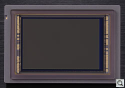
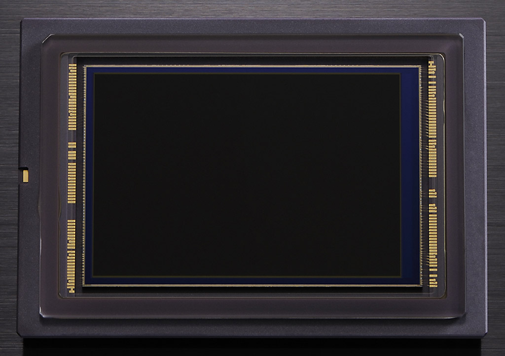
Nope.I can't find the name of the manufacturer of Nixon"s sensor in the spec, unlike Canon or Sony which is written by Canon or Sony. I think a lot of Nikonians want to know. Please tell us if any one knows. Thank you.(I hope it is made by Nikon I will be glad).
I'm wondering if we know the same guy :?That, unfortunately, I can't reveal. You are correct, Renesas is leaky.I'd be interested in knowing the nature of the leak, Renesas is quite leaky, in my experience.
On the one hand, there was never any chance that the D3 would have had anything other than a new sensor, each new Dx has had. I suppose you're saying he got basic unexpected details right, like FF (although that was expected by many) and CMOS (although that was to be expected after the D2x) or 12 channel analog output. My guy seems to know quite a lot about the innards of both Canon and Nikon cameras, one of the reasons being that they have contact with the mules in the dev labs. Of course, under strict NDA, but different individuals have diffferent approaches to those (and I've never heard anything until after a product's been released).But I will say that part of the leaked information I received was about a "new imaging sensor in the D3." As it turns out, the information was basically correct (and about 12 months prior to the announcement).
True, most rumours are very poorly informed.What confused me at the time and made me discount it was this "leak" didn't match any of the other rumors or leaks that were circulating.
I suspect the most likely circumstance is to do with Mitsubishi Semiconductor background. MS was merged into Renesas, and was also instrumental in developing the Canon sensor line. If there was an individual, or group of individuals from or ex MS (or even currently employed by Renesas) who had participated in the Canon project, who better for Nikon to turn to? The D3 sensor certainly has canon-like design features.Hard for me to say, as I don't have the experience they do. But there's another possible answer: Renesas was in some way involved in the sensor partnership (i.e. it was at least a three-way). But the more I think about, I think you're right: Chipworks is probably overinterpreting tools and design style clues.That was one of the bits of evidence that Chipworks gave. Whether this is a real clue depends on what the nature of the 'markings' they are talking about.Second, the markings on the sensor look like Renasas labeling.
How, then, do you account for the differences between the D3x and D3 sensors? To anyone with a clue of modern mass-production rules, it is clear that they are products of different design teams and plants/Nope.I can't find the name of the manufacturer of Nixon"s sensor in the spec, unlike Canon or Sony which is written by Canon or Sony. I think a lot of Nikonians want to know. Please tell us if any one knows. Thank you.(I hope it is made by Nikon I will be glad).
It is quite obvious for me and any person having clue of modern "mass-production" rules that it is SONY.
Actually, the CFA is stronger (better colour separation). Every camera manufacturer puts in their own AA filter. It's not part of the sensor.Nevertheless. Nikon puts it's own weaker CFA as well as AA-filter on top
Of course, he doesn't say how long. Over on another thread, I've been arguing that a 24MP/10FPS D4, with a Nikon sensor, is a possibility, since it would allow a repeat of the D3 trick, replace both the low and high res versions of the previous generation with a single camera to allow time to develop a new high res sensor. Another possibility, given that the D3s still seems pretty competitive against the 1DIV, would be to release the D4x, with a Nikon sensor, first. The advantage of that is that the small sensel design would be available for the DX line of cameras, the sensors for which could be engineered quite fast (assuming that designing a really good sensel is the thing that takes the time). It will be interesting to see what they do do, but 'we plan on merging them' seems a pretty clear statement of intent.I'm not so sure about that. It seems logical, true, but there are economic implications in going it alone, especially at the low end. I'd bet that Nikon gets to an all-Nikon FX lineup long before it leaves Sony at the low end.Which says to me 'bye-bye, Sony'."we currently have two sensor sources: internally developed and external sourced and we plan on merging them".
If my Toshiba speculation is right, then it looks like they're doing the same again.This would be my reading, too. Indeed, this is basically a continuation of what I've been saying for some time. The stories that finally surfaced about the D1/D1h/D1x sensor development seem to indicate that Sony wasn't particularly interested in doing such APS sensors at the time, but Nikon directed some specific work by Sony, which is how we got a binned 10mp sensor in the D1 and the partially-binned D1x sensor.
Not sure, the A900/D3x sensel seems to perform about as well as the D3. The key to the D3's performance is keeping the photoelectron density quite low, and the efficiency high (which took 2 element microlenses - Nikon calls them 'inner lenses' - to get a gapless design with such large pixels). It compromises base DR a little, but means that the camera is running 1 stop ahead of the Canons. According to measurements, the read noise was about twice Canon's for both the D3 and d3x (4.9 plays 2.5 e-). I suspect what has happened with the D3s is that they have got read noise down to canon levels, while retaining the high base ISO advantage.Agreed. Which rules out Sony, I think. Sony was a bit late to the CMOS game--I don't think the D3 sensor could have derived from Sony's CMOS work to date.
I'm not sure they're reluctant to market the D3 sensor - they put out a lot of information about it. They've been much more circumspect about the d3x sensor, mainly because I suspect the chip is an off-the-shelf Sony. But, the microlenses and CFA are a very important part of a sensor, as well as the silicon, and Nikon has shown it knows how to sequence the data acquisition and do the signal processing to get much more out of sony chips than Sony does.Yes, true. But the sensor is at the heart of what makes a digital camera what it is. You have to figure out a way to market that. If that means that your marketing has to say "the right partnerships make a better sensor than going it alone" then that's what you do. Nikon seems reluctant to truly market the sensor, yet they've got arguably the best sensor going. This is a strange position to put yourself into. It gets perceived as a weakness, not a strength.
Me too. Particularly if Nikon has decided its rrelationship with Sony is difficult, my guess is that it would want to hang on to all the IP in its sensors, which means having a design team working for Nikon (on whatever contractual basis) doing the work. If it included any Tosh IP in the designs, it would be back where it is with Sony. Moreover, currently Tosh is only active in camphone sensors, so long as Nikon holds the IP, there is no possibility of the sensors turning up in other vendors' cameras (as the IMX021 has with Leica, Ricoh and Pentax). While it inevitably has to design to process, at least it is in a position with three fab lines offering compatible processes. I suppose it's possible that Tosh might decide to go into commodity DSLR sensors, or move into the DSLR business, but I should think unlikely. And if it does, there's always IBM.After thinking about it more, I'd say your Toshiba guess is possibly correct for a fab. The real question would be whether the gains in the sensor are Toshiba-based, Nikon-based, Toshiba+Nikon-based, or whether there's additional partnership in the mix. I'd bet on the latter.
I just got the official transcript of the Q&A session from Nikon and here is the official sanctioned version:The second question was from me and I asked what does it mean when Nikon said the D3/D700/D3S sensor is developed by Nikon. Is it same meaning as the D2H LBCAST? The anwser was very strange but very typical Japanese when they don't want to answer your question directly: "CMOS sensors are used by many camera manufacturers and there are advantages in the CMOS design. In the case of D3/D3S Nikon specificies the parameters of pixel and the overall sensor behavior."
Another way to look at it is which Sony sensors Nikon has elected skip . I can count two of them:I find that an interesting answer because I suspect any "merger" was already in progress before the D3 appeared. Right now Nikon uses four sensors in DSLRs:
10mp DX: Sony
12mp DX: Sony-derived
12mp FX: Nikon
24mp FX: Sony-derived
The real question is what the next sensor will be. Nikon needs a higher count DX and higher count FX sensor for next generation products. My bet would be that we see another Nikon-designed FX sensor sooner rather than later. This would be consistent with their top-down approach on technology. If they can get the high-end right, they can then look to push that down into the prosumer and consumer products.